The rapid development of artificial intelligence technology has made generative AI the core direction of current development. Introducing generative AI into smart devices, especially portable smart terminals, is seen as an inevitable trend in future technological development. Smartphones, as one of the most important terminals, are becoming the pioneering platform for generative AI applications.
Generative AI places high demands on flash memory, particularly in terms of data processing speed and transmission efficiency. The highest flash memory standard currently is the UFS 4.0 standard released by the JEDEC Association in 2022, which has doubled the transmission speed compared to the previous generation. It is believed to be a standard feature for flagship smartphones and the next generation of AI phones. The Charging Head Network has compiled the main parameters of each generation of UFS into the table below for a more comprehensive understanding.
Sequential read and write speeds may vary due to different devices, testing environments, and optimizations by chip manufacturers, so the above are all theoretical parameter ranges, and the data is for reference only.
Against this backdrop, major storage control chip manufacturers have also accelerated their layout of UFS 4.0 solutions.
Summary of UFS 4.0 Main Control Chips
The Charging Head Network has compiled some known UFS 4.0 main control chips currently available on the market into the table below for your selection and understanding.
The ranking is not in order and is sorted by the first letter of the company’s English name.
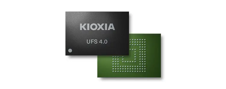
KIOXIA’s latest generation of UFS 4.0 flash memory chips offers capacity specifications of 256GB, 512GB, and 1TB. This chip uses KIOXIA’s BiCS Flash 3D flash memory and controller, integrates MIPI M-PHY 5.0 and UniPro 2.0, and supports a theoretical interface speed of 23.2 Gbps per channel or 46.4 Gbps per device, and is backward compatible with UFS 3.1.
Compared to the previous generation UFS 4.0 products, the new flash memory chip has a 15% increase in sequential write speed, a 50% increase in random write speed, a 30% increase in random read speed, and the sequential read speed remains unchanged at 4640MB/s. Additionally, the new product uses a JEDEC standard package of 9mm×13mm, which is 18% smaller than the previous generation’s 11mm x 13mm package, with a thickness of 0.8mm for the 256GB and 512GB flash memory packages, and 0.9mm for the 1TB package.
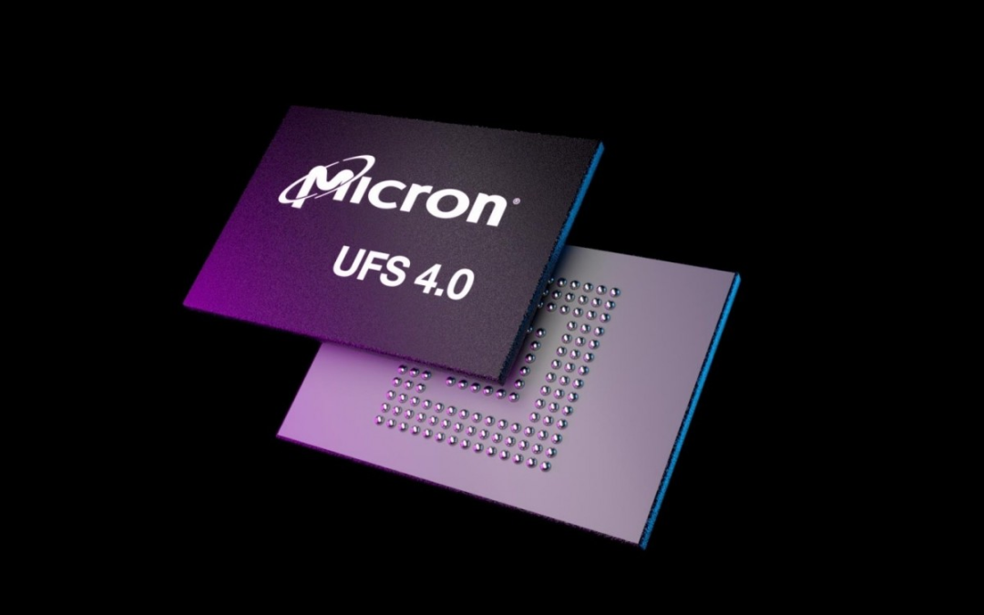
This storage is built on 232-layer 3D NAND technology, measuring only 9×13mm. Compared to the 11×13mm storage solution released in June last year, the former’s size has been reduced by 20%, while performance has not been affected. This storage offers a maximum space of 1TB, with sequential read speeds reaching 4300MB/s and sequential write speeds reaching 4000MB/s.
The PS8361 targets the highest specifications of the flagship smartphone market, belonging to the UFS 4.0 control chip, manufactured using a 12nm process, designed for four channels, with a maximum flash memory capacity of 1TB, equipped with sixth-generation LDPC+RAID ECC error correction technology, and sequential read and write speeds exceeding 4000MB/s. With its improved reading performance per unit mA, it will effectively extend the battery life of mobile devices.
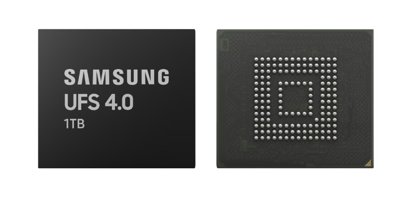
The newly developed UFS 4.0 by Samsung uses Samsung’s seventh-generation V-NAND and proprietary controller, achieving sequential read speeds of 4200 MB/s and sequential write speeds of 2800 MB/s, which are approximately 2 times and 1.6 times that of the previous generation UFS 3.1, respectively. Energy efficiency has also been significantly improved. Samsung’s new UFS 4.0 can provide up to 6.0 MB/s of sequential read speed per milliamp (mA), a 46% increase over UFS 3.1, allowing smartphones to have longer battery life with the same battery capacity.
Samsung UFS 4.0 has added an advanced Replay Protected Memory Block (RPMB). With this design, the storage efficiency for important personal data that can only be read or written after authentication is improved by 1.8 times. This new mobile storage solution is extremely compact, with a maximum size of 11mm x 13mm x 1mm, and a maximum capacity of up to 1TB.
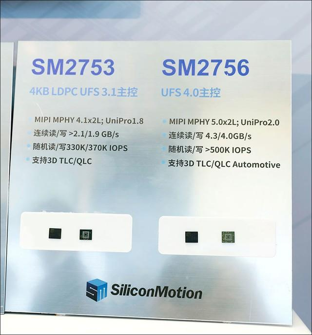
The SM2756 main control chip can be regarded as one of the most advanced UFS 4.0 main control solutions currently available, based on 6nm EUV process technology, featuring a dual-channel design, utilizing MIPI M-PHY low-power architecture, achieving a perfect balance between performance and power consumption, meeting the needs of today’s top AI mobile devices for 24-hour computation.
In terms of performance, the SM2756 can provide over 4,300MB/s sequential read speed and over 4,000MB/s sequential write speed, while supporting the latest 3D TLC and QLC NAND flash technologies and handling storage capacities of up to 2TB.
Charging Head Network Summary
The rapid development of generative AI technology is constantly increasing the storage performance demands of smart devices. UFS 4.0, as the forefront standard of current storage technology, is gradually becoming standard for smart terminals.
UFS 4.0 not only significantly improves transmission speeds but also optimizes power consumption control and data security, enabling devices such as smartphones and tablets to achieve higher efficiency and battery life when processing generative AI tasks. By adopting more advanced process technologies and NAND flash architectures, these main control chips can provide higher performance for devices, meeting the stringent demands of the future AI era.
Click on the blue text to learn more about the following popular topics, or reply with the keywords below in the Charging Head Network WeChat backend to access the special topics.
「Annual Teardowns」
2024、2023、2022、2021、2020、2019、2018、2017、2016、2015
「Teardown Categories」
Outdoor Power Supplies、Inverters、Charging Guns、Charging Piles、Server Power Supplies、PC Power Supplies、Chargers、Power Banks、Wireless Chargers、Car Chargers、Charging Cables、Power Strips、Inflatable Treasure、Hair Dryers、Car Inverters、Electric Toothbrushes、Docking Stations、Inflatable Treasure、Cooling Back Clips、V Port Batteries、Mobile Wi-Fi、Small Fans、Electric Mosquito Swatters、Flashlights、Displays、Power Tools
「Application Cases」
South Chip、Yingjixin、Zhirong、Beiyiwei、Meixinsheng、Jiahua Te、Maoruxin、Huayuan、Silicon Power、Tian Deyu、Dongke、Xinhai、Yichong、Qinheng、Yutai、Chengxinwei、Hengchengwei、Xinjing Electronics、Tereixin、Wode、Yingnuoseke、Nitride、Weizhao、Yuhongjin、Chuan Tu Micro、AOS International、Matsuda


