
The invention of the vacuum tube was a significant driving force in the development of the electronics industry. However, after World War II, the need for a large number of discrete components significantly increased the complexity and power consumption of devices, while their performance continuously declined. One example is the Boeing B-29, which consisted of 300 to 1000 vacuum tubes. Each additional component reduced system reliability and increased troubleshooting time.
A major breakthrough occurred in 1947, coming from John Baden, William Shockley, and Walter Brattain at Bell Labs, who invented the germanium transistor. In 1950, Shockley developed the first bipolar junction transistor (BJT). Compared to vacuum tubes, transistors are more reliable, more efficient, and smaller in size.
In 1958, Jack Kilby of Texas Instruments built the first integrated circuit, consisting of two bipolar transistors connected on a single silicon chip, thus starting the “Silicon Age”.
Early ICs used bipolar transistors. However, the static power consumption of BJTs presented a significant problem. This meant that even when the circuit was not turned on, current would still flow. This limited the number of transistors that could be integrated into a single silicon chip.
In 1963, Frank Wanlass and CTSah of Fairchild Semiconductor announced the first logic gate, which used n-channel and p-channel transistors in a complementary symmetry circuit configuration. This is what is now known as CMOS, which has almost zero static power consumption.
In the following years, improvements in CMOS processing led to increased circuit speeds and further improvements in chip packaging density and cost-effectiveness.
Below, we will discuss Bulk-Si CMOS technology, SOI, and FinFET, along with related solutions. We will also discuss the physical size limitations of transistor materials and the new materials used in advanced technology nodes.
Overview of MOSFET
Here, we first discuss the core unit of CMOS, which is the basic structure and important terms of the MOSFET or simply MOS.
MOS Structure
MOS is mainly divided into two structures based on the channel type: n-channel and p-channel MOS. Here, we will only outline the NMOS transistor.
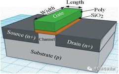
MOS transistors are four-terminal devices with a drain, source, gate, and substrate. Figure 1 shows the 3D structure of NMOS. The NMOS transistor is formed on a p-type silicon substrate (also known as the body). A low resistivity electrode is formed at the top center of the device, separated from the body by an insulator. Typically, n-type or p-type heavily doped polysilicon is used as the gate material. Here, silicon dioxide (SiO2 or simply oxide) is used as the insulator. By implanting donor impurities on both sides of the substrate, the source and drain are formed. In Figure 1, these regions are indicated by n+, representing heavy doping of donor impurities. This heavy doping results in low resistivity in these regions.
If the two n+ regions are biased at different potentials, the lower potential n+ region will act as the source, while the other will act as the drain. Therefore, the drain and source terminals can be interchanged based on the potentials applied to them. The region between the source and drain is referred to as the channel, which has a width-W and length-L, playing a crucial role in determining the characteristics of the MOS transistor.
Figure 1. Structure of NMOS Transistor
Why Use Polysilicon as Gate Material?
In the early semiconductor industry, aluminum metal was commonly used as the preferred gate material for MOS. However, later, polysilicon was chosen as the gate material for two main reasons.
The early MOS manufacturing process began with the definition and doping of the source and drain regions. Then, a gate mask was used to define the gate oxide region for forming the aluminum metal gate.
One of the main drawbacks of this manufacturing process is that if the gate mask is misaligned, it produces parasitic overlapping input capacitances Cgd and Cgs, with Cgd being more detrimental due to feedback capacitance. As a result of milling capacitance, the switching speed of the transistor is reduced.
Another reason for choosing polysilicon is that the threshold voltage of the MOS transistor is related to the difference in work function between the gate and the channel. Previously, when the operating voltage was in the range of 3-5V, metal gates were used. However, as transistors shrank, it ensured that the operating voltage of the device also decreased. Transistors with this high threshold voltage became inoperable under these conditions. The use of metal as a gate material resulted in a higher threshold voltage compared to polysilicon because polysilicon would have a composition similar to that of the body Si channel. Additionally, since polysilicon is a semiconductor, its work function can be modulated by adjusting the doping level.
Continuous Evolution of Technology
The market demand for battery-powered portable electronics is increasing, including hearing aids, mobile phones, laptops, etc., which require lower power consumption and cheaper development. For these portable devices, power consumption is a critical metric since the power provided by batteries is quite limited. Unfortunately, battery technology cannot be expected to increase battery storage capacity by more than 30% every five years. This is insufficient to address the increasing power consumption in portable devices.
In 1965, Gordon E. Moore predicted that the number of transistors in integrated circuits would double every two years (the well-known Moore’s Law). By making transistors smaller, more circuits can be manufactured on a silicon wafer, thus making circuits cheaper. Reducing the channel length allows for faster switching operations because the current takes less time to flow from the drain to the source.
For long-channel devices, the “edge effect” at the edges of the channel can truly be neglected. For long-channel devices, the electric field lines are perpendicular to the surface of the channel. These electric fields are controlled by the gate voltage and back-gate voltage. However, for short-channel devices, the drain and source structures are closer to the channel, especially when the longitudinal electric field enters the channel. The longitudinal electric field is controlled by the drain-source voltage. The longitudinal electric field is parallel to the direction of current flow. If the channel length is not greater than the total depletion width of the source and drain, the device is referred to as a short-channel device.
Due to the two-dimensional potential distribution and high electric fields in short channels, various adverse effects occur.
Carrier Velocity Saturation and Mobility Degradation
The drift velocity of electrons in the channel is proportional to the electric field value at lower electric fields. These drift velocities often saturate at high electric fields. This is called velocity saturation. For short-channel devices, the longitudinal electric field usually also increases. At such high electric fields, velocity saturation occurs, affecting the I-V characteristics of the MOSFET. For the same gate voltage, the saturation mode of the MOSFET is achieved at lower drain-source voltage values and with reduced saturation current.
Due to the higher vertical electric field, carriers in the channel leave the oxide interface. This leads to a reduction in carrier mobility and a decrease in drain current.
Hot Carrier Effects
For smaller geometry devices, the electric field especially increases near the drain. As a result, electrons gain a significant amount of energy known as hot carriers.
Some of these gain enough energy to cause collision ionization near the drain, generating new electron-hole pairs, which produce drain-bulk current (Idb). A small number of hot electrons can cross the oxide and be collected through the gate. While some hot carriers may even damage the oxide, leading to device degradation.
Above, only two adverse effects have been listed, and there are other effects that are not discussed here.
How to Address Short Channel Effects?
If the channel length is small compared to the depletion region, short channel effects become intolerable. This limits further reduction in gate length. To mitigate these effects, the depletion region width should decrease as the channel length decreases. This can be achieved by increasing the channel doping concentration or increasing the gate capacitance.
The gate capacitance determines the gate’s control over the channel. Equation 1 indicates that the gate capacitance can be increased by reducing the thickness of the gate oxide. Devices with thinner gate oxides have reduced depletion widths, thus improving SCE characteristics.
Cox = EOX / TOX (Equation-1)
Here: Cox is the gate oxide capacitance, EOX is the oxide electric field, TOX is the oxide thickness.
For Intel’s process nodes over the past 25 years, to limit SCE, the oxide has been roughly proportional to the channel length. The relationship between channel length and oxide thickness for Intel technology nodes is shown in Equation 2.
L = 45 x TOX (Equation-2)
Here: L is the channel length, TOX is the oxide thickness.
Improvements in Traditional Architecture
High-K Dielectrics Reduce Leakage
The thickness of the SiO2 dielectric should be proportional to its channel length. The 65nm node requires about 2.3nm of effective oxide thickness (EOT) (actual 1.6nm). However, if the oxide thickness is further reduced below this point, the direct tunneling of carriers will dominate, and gate leakage will increase to unacceptable limits. Therefore, the oxide thickness limit is about 1.6nm, set by the tunneling leakage from the gate to the channel (also known as quantum mechanical tunneling).
If we look at Equation 1, the only option is to choose dielectric materials with high dielectric constants (K) to increase the oxide capacitance. Since a thicker dielectric layer can be used, higher gate oxide capacitance is achieved. Thicker layers lead to less carrier tunneling. The dielectric constant of SiO2 is 3.9.
A breakthrough in gate oxide was achieved in 2007 with hafnium (HfO2)-based high-K dielectric materials, first introduced by Intel in its 45nm high-volume manufacturing process. The dielectric constant of hafnium materials is about 25, which is six times higher than that of SiO2.
EOT is given by Equation 3. Equation 3 means that a 6nm thick HfO2 provides about 1nm of EOT.
EOT = (3.9 x TOX) / K (Equation-3)
Here: EOT is the effective oxide thickness, TOX is the oxide thickness, K is the dielectric constant of the material.
Strained Silicon Technology
One of the key scaling issues for nanoscale transistors is mobility degradation caused by larger vertical electric fields. There are many methods to enhance the performance and mobility of transistors. One method is to use thin germanium films in the channel, as germanium has higher carrier mobility. Another method is to use strained silicon by introducing mechanical strain in the channel.
Strained silicon technology involves physically stretching or compressing the silicon crystal through various means, which in turn increases carrier (electron/hole) mobility and enhances transistor performance. For example, when the channel is under compressive stress, the hole mobility of PMOS can be increased.
To generate compressive strain in the silicon channel, Si-Ge films are filled in the source and drain regions through epitaxial growth. Si-Ge typically contains a mixture of 20% germanium and 80% silicon.
The number of Si and Ge atoms equals the original Si atoms. Germanium atoms are larger than silicon atoms. Therefore, when a force is created, it pushes the channel and increases hole mobility. Improved semiconductor mobility enhances drive current and transistor speed.
MOS transistor strained silicon technology was first used in the 90nm process in 2003. At this technology node, the Si-Ge source-drain structure used for PMOS transistors induced compressive strain in the channel, increasing the current by 25%. While NMOS strain was introduced by adding a high-stress Si3N4 capping layer around the transistor, it increased the current by 10%.
Metal Gate Addresses Poly-Silicon Depletion
A depletion region forms at the interface of polysilicon and gate oxide, which increases as the device continues to shrink, and a significant portion equivalent to the oxide thickness limits the gate oxide capacitance. The negative impact of poly-depletion is due to the reduction of inversion layer charge density and degradation of device performance. Therefore, in addition to minimizing the thickness of the gate oxide, the depletion layer thickness of polysilicon also needs to be minimized.
One solution to eliminate poly-depletion effects is to use a metal gate instead of a polysilicon gate. Metal gates not only eliminate poly-depletion effects but also allow for the use of high-K dielectrics.
Intel first introduced high-K dielectrics and metal gate technology at the 45nm node. Different metals are used for NMOS and PMOS as NMOS and PMOS require different functionalities.
Innovative Structures
For traditional MOS structures, as the channel length decreases, the gate cannot fully control the channel, which is undesirable. One of the effects is increased subthreshold leakage from the drain to the source, which is not favorable from a power consumption perspective.
In conventional MOS, the gate cannot control the leakage paths far from it. Various MOS structures that allow transistors to scale beyond the conventional MOS scaling limits can be used for improvements.
Below, we will discuss two new MOS structures, namely FinFET and SOI. The primary goal of adopting these two structures is to maximize gate-to-channel capacitance and minimize drain-to-channel capacitance.
FinFET
The concept of FinFET was proposed in 1999 by Dr. Chang-Goo Lee, the former CTO of TSMC, and his team, with UTB-SOI (FD SOI) proposed in 2000. Both structures are thin-body, allowing the gate capacitance to be closer to the entire channel, with the body being thin, about 10nm or less. Therefore, there are no leakage paths far from the gate. The gate effectively controls leakage.
Modern FinFETs are three-dimensional structures, as shown in Figure 2, also known as tri-gate transistors. FinFETs can be implemented on bulk silicon or SOI wafers. The FinFET structure consists of thin (vertical) fins of silicon on the substrate. This channel provides excellent three-dimensional control of the channel. This structure is called FinFET because its Si body resembles the tail fin of a fish.
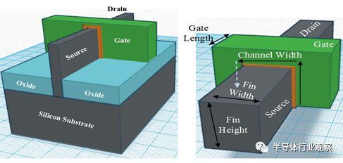
Figure 2. Fin-FET Structure
In bulk-MOS (planar structure MOS), the channel is horizontal. In FinFET, the channel is vertical. Thus, for FinFET, the height of the channel (fin) determines the width of the device. The perfect width of the channel is given by Equation 4.
Channel Width = 2 x Fin Height + Fin Width (Equation-4)
FinFET technology offers many advantages over bulk CMOS, such as higher drive current for a given transistor aspect ratio, higher speed, lower leakage, lower power consumption, and no random dopant fluctuations, thus ensuring better mobility and size of transistors above 28nm.
In conventional MOS, doping is inserted into the channel to reduce various SCE and ensure high Vth. In FinFET, the gate structure is wrapped around the channel, and the body is thin, providing better SCE, thus channel doping is optional. This means FinFET is less affected by dopant-induced variations. Low channel doping also ensures better mobility of carriers within the channel. Therefore, performance is higher. It is noteworthy that both FinFET and SOI technologies consider Body Thickness as a new scaling parameter.
Silicon on Insulator (SOI)
The main difference between traditional MOS structures and SOI MOS structures is that SOI devices have a buried oxide layer that isolates the substrate from the body. As shown in Figure 3, SOI transistors are planar structures.
The manufacturing process of SOI MOS is similar to that of body MOS (traditional MOS) outside the starting silicon wafer. SOI wafers consist of three layers: 1. A thin surface layer of silicon (forming the transistor); 2. An insulating material layer; 3. A supporting or “handling” silicon wafer.
The basic idea of the buried oxide layer is to reduce parasitic junction capacitance. The smaller the parasitic capacitance, the faster the transistor operates. Due to the BOX layer, there are no leakage paths far from the gate, leading to lower power consumption.
Typically, SOI devices are classified as partially depleted (PD) SOI and fully depleted (FD) SOI. Compared to PD-SOI, FD-SOI has a very thin body structure, thus fully depleting during operation. FD-SOI is also known as ultra-thin body SOI. For PD-SOI, the body thickness is 50nm to 90nm. For FD-SOI, the body thickness is about 5nm to 20nm.
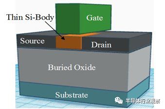
Figure 3. Structure of SOI FET
Advantages of SOI Devices:
-
Reduced leakage/source parasitic capacitance due to the oxide layer. Therefore, compared to bulk CMOS, the device’s delay and dynamic power consumption are lower.
-
Due to the oxide layer, the threshold voltage is less dependent on back-gate bias compared to bulk CMOS. This makes SOI devices more suitable for low-power applications.
-
SOI devices have better subthreshold characteristics and lower leakage currents.
-
SOI devices do not have latch-up issues.
Disadvantages of SOI Devices:
-
One of the drawbacks of PD-SOI devices is that they exhibit history effects. In PD-SOI, as the body becomes thicker, the floating body effect is significant. Therefore, the body voltage depends on the previous state of the device. This floating body voltage can change the threshold voltage of the device. This may lead to significant mismatches between two identical transistors.
-
Another issue with SOI devices is self-heating. In SOI devices, the active thin body is on the silicon oxide, which is an adiabatic material. During operation, the power consumed in the active region cannot easily dissipate. As a result, the temperature of the thin body rises, reducing the mobility and current of the device.
-
One of the challenges of FD-SOI is the difficulty in manufacturing thin body SOI wafers.
Which is Better: FinFET or SOI?
Since SOI technology is very close to planar bulk silicon technology, it requires little investment for fabs. Therefore, existing bulk technology libraries can easily transition to SOI libraries. Another advantage of SOI over FinFET is the good back-gate bias options. By creating a backdoor region beneath the BOX, Vt can be controlled. This makes it suitable for low-power applications.
The main limitation of SOI technology is that the cost of wafers is higher than that of bulk silicon wafers because it is very difficult to control the silicon film on the entire wafer. Another stumbling block for SOI adoption is the limited number of SOI wafer suppliers. Intel states that SOI wafers account for about 10% of the total process cost.
Compared to SOI, FinFET has higher drive currents. Additionally, in FinFET, strain technology can be used to increase carrier mobility.
One of the drawbacks of FinFET is its complex manufacturing process. Intel states that the cost of manufacturing FinFET is 2-3% higher than bulk silicon.
Intel introduced Trigate FET at the 22nm node of the Ivy-Bridge processor in 2012. Other foundries providing FinFET technology include TSMC, Global Foundries, and Samsung. In 2014, TSMC released its first fully functional ARM-based 16nm FinFET technology network processor.
STMicroelectronics released its first FD-SOI chip for mobile processors at 28nm technology in 2012. Vendors providing FD-SOI technology include IBM, Global Foundries, and Samsung. Additionally, some AMD processors, PowerPC microprocessors, and Sony’s PlayStation also use SOI technology.
Future Technology Trends
Both FinFET and SOI structures have better gate control and lower threshold voltages, resulting in less leakage. However, as we move towards low technology nodes below 10nm, leakage issues re-emerge, leading to many other problems such as threshold flattening, increased power density, and heat dissipation.
FinFET structures are less efficient in thermal dissipation because heat tends to accumulate on the fins. These issues may lead to a new class of design rules – Thermal Design, unlike other design rules such as “Design for Manufacturability.” As these devices approach, eInfochips is collaborating with academia to provide potential solutions, including modifying device structures and replacing existing silicon materials with new materials. Among these, carbon nanotube (CNT) FETs, hybrid semiconductor gate-all-around nanowire FETs or FinFETs may prove to be promising solutions in future technology nodes.
Moreover, in recent years, Samsung and TSMC have been racing ahead in semiconductor processes, continuously pushing the industry’s focus. Recently, at the Samsung Foundry Forum SFF 2018 USA held in the US, Samsung announced its continuous advancement into 5nm, 4nm, and 3nm processes, approaching physical limits!
According to Samsung’s plans, its 4nm process will still use existing FinFET manufacturing technology, but by the 3nm process node, Samsung will abandon FinFET technology in favor of GAA (Gate-All-Around) nanoscale technology.
Gate-All-Around means the gate surrounds the channel, which will redesign the underlying structure of the transistor, overcoming the physical and performance limits of current technologies, enhancing gate control, and significantly improving performance.
Samsung’s GAA technology is called MBCFET (Multi-Bridge Channel Field Effect Transistor), which is currently under development using nanoscale devices.
New Processes like GaN
In the future, silicon will continue to dominate semiconductor manufacturing; however, more and more designers are turning to alternative semiconductors as materials and manufacturing processes become more affordable. These materials mainly include compound semiconductors such as silicon carbide (SiC), indium gallium phosphide (InGaP), indium phosphide (InP), and gallium nitride (GaN). Among them, GaN has already begun to yield significant benefits, especially in applications that require high speed, high frequency, high efficiency, thermal resistance, and high power.
In addition to silicon devices, circuits using new materials and manufacturing processes have achieved breakthroughs, such as devices made from GaN. These materials have created some interesting new types of transistors.
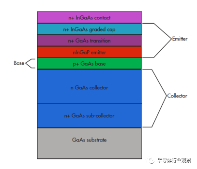
Figure 4: The structure of InGaP HBT shows the GaAs substrate with collector, base, and emitter layers. The resulting transistor has high gain at lower microwave frequencies, below 20 GHz.
GaAs or GaN substrates can be used to manufacture any type of transistor, including the most popular bipolar junction transistors (BJT) and enhancement-mode MOSFETs. Other types of transistors have also emerged, such as heterojunction bipolar transistors (HBT), MESFETs, HEMTs, etc. These utilize the characteristics of substrate materials to produce optimal amplification and power handling capabilities.
HBT uses a standard BJT configuration but employs different base and emitter materials. A popular combination is a GaAs emitter and an AlGaAs base. As a result, very high gains are achieved at microwave frequencies of up to 250 GHz. Figure 4 shows the complex structure of InGaP HBT. This combination can be used for microwave power amplifiers.
MESFET, or Metal-Semiconductor FET, is essentially a JFET with a metal gate for forming Schottky junctions with the dominant channel. It provides depletion mode, where the device is normally on and turned off by applying a negative gate voltage. MESFETs are typically made from GaAs and have high gain at microwave frequencies.
A variant of MESFET is the High Electron Mobility Transistor (HEMT), also known as Structure FET (HFET) or Modulation-Doped FET (MODFET). It is typically formed with GaAs or GaN with additional layers and Schottky structures (Figure 5). The depletion mode is the most common configuration. An improved performance version uses pHEMT with an additional indium layer to further accelerate electron movement. These devices operate at frequencies of 30 GHz or higher.
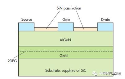
Figure 5: This is the basic structure of GaN HEMT. The substrate is usually sapphire or silicon carbide, but silicon can also be used. 2DEG represents a two-dimensional electron gas, a layer of gas made up of electrons that can move vertically in any direction.
Recently, GaN has been used to create standard normally-off enhancement-mode MOSFETs. These devices can operate at voltages of up to several hundred volts with very low on-resistance. These GaN-on-Si devices target switch-mode power supply applications.
GaN transistors have been used in military systems for some time, about 10 years. Under the initiative of the US Department of Defense (DoD), GaN has rapidly developed into the latest star technology for microwave power amplifiers. Initially developed for improvised explosive devices (IEDs) for the Iraq War, GaN has now appeared in all new microwave and millimeter-wave electronic products, including radar, satellites, communications, and electronic warfare (EW) systems.
What makes GaN so impressive is its high power density, while GaAs has a fundamental power density of about 1.5W/mm, GaN has a power density of 5 to 12W/mm. It also has high electron mobility, meaning it can amplify signals well into the higher GHz range. Typical GaN transistors have an fT of 200 GHz. Additionally, it can achieve relatively high breakdown voltage levels, reaching about 80V.
GaN devices are typically manufactured on two different substrates, GaN on silicon or GaN on silicon carbide (SiC). Among these two types, the general consensus is that lower power devices use the cheaper Si substrate. High power devices with better thermal performance should use SiC substrate wafers.
The downside of GaN is its high cost. Current costs are decreasing as more suppliers enter the market and usage increases. These materials are expensive, and the costs of the manufacturing processes and equipment are high. As quantities increase further, production costs will decrease, but will still remain above the cost levels of CMOS processes.
The main application focus of GaN technology is microwave and millimeter-wave power amplifiers. A single amplifier can reach power levels of dozens of watts. In other parallel/push-pull/Doherty configurations, power levels of hundreds or even thousands of watts are possible, with most applications being military-related phased array radar modules, satellite power amplifiers, jammers, and other electronic warfare (EW) devices.
In the past, traveling wave tubes (TWTs) achieved high power, and today they remain a choice for some applications. After the emergence of silicon LDMOS FETs, which provide power levels of hundreds to thousands of watts. However, these devices cannot be used at frequencies above 6 GHz. The demand for high-power in the microwave and millimeter-wave bands has driven the development of new GaN transistors, which can easily provide dozens to hundreds, or even thousands of watts at frequencies of 30 GHz or higher in just a few years.
It is predicted that GaN amplifiers will begin to replace some TWT satellite and radar amplifiers. For power conversion, GaN also has significant advantages. GaN transistor switches operate at high voltages, making them ideal for high-power DC-DC converters and other switch-mode circuits. In some applications, GaN switching transistors can replace IGBTs. GaN devices can achieve smaller sizes, more efficient and thermally resistant circuits, which are essential for military applications.
GaN is also suitable for applications beyond power amplification or conversion. GaN can be used to create different types of transistors, such as MESFETs, HBTs, and pHEMTs. These can be used to manufacture MMIC amplifiers. With the improvement of these new devices, they will gradually replace silicon as they can operate stably at frequencies of 40 GHz.
GaN manufacturing processes are continually advancing to reduce costs. Currently, GaAs continues to dominate, mainly used for small signal MMICs, LNAs, and low-level power amplifiers for mobile and wireless radios. However, as GaN costs decrease and GaN penetrates small signal application areas, gallium arsenide is likely to lose significant market share, while others using silicon (LDMOS), SiGe, and SiC will continue to find their unique niche applications.
Conclusion
Since the 1960s, the semiconductor industry has been chasing Moore’s Law, which states that the number of transistors on a chip doubles every two years (or 18 months). Transistor sizes have decreased, speeds have increased, and more circuits can be placed on a smaller chip.
Looking to the future, there are two main issues:
First, the feature sizes of transistors have reached atomic sizes in materials, which is the ultimate limit. Currently, 10nm chips are being manufactured, and some manufacturers are researching even smaller 7nm to 5nm processes. Producing such chips is comparatively difficult and expensive, meaning that only the largest and most equipped semiconductor manufacturers can develop chips based on smaller geometries.
Second, how will the semiconductor industry grow? Silicon products will continue to exist, and new opportunities such as automotive electronics and Internet of Things (IoT) devices will arise. The mobile phone industry still requires standard chips as well as faster chips. Therefore, more and more new materials and processes will be adopted.
This article is sourced from: Semiconductor Industry Observation