
Basic Concepts of RF Power Amplifiers
RF power amplifiers (RF PA) are a crucial part of the transmission system, and their importance is self-evident. In the front-end circuit of the transmitter, the RF signal power generated by the modulation oscillator is very small and needs to be amplified through a series of stages (buffer stage, intermediate amplification stage, final power amplification stage) to obtain sufficient RF power before being fed to the antenna for radiation. To achieve sufficiently high RF output power, RF power amplifiers must be used. After the modulator generates the RF signal, the RF modulated signal is amplified to sufficient power by the RF PA, matched through a matching network, and then transmitted by the antenna.
The function of an amplifier is to amplify the input content and output it. The input and output content is referred to as “signal,” often represented as voltage or power. For an amplifier as a “system,” its “contribution” is to elevate what it “absorbs” to a certain level and “output” it to the outside world. If the amplifier can perform well, it can contribute more, reflecting its own “value.” If there are certain problems with the amplifier, it may not only fail to provide any “contribution” after starting or after a period of operation but may also exhibit some unexpected “oscillations,” which can be catastrophic for both the outside world and the amplifier itself.
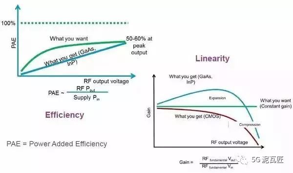
The main technical indicators of RF power amplifiers are output power and efficiency. How to improve output power and efficiency is the core of the design goals for RF power amplifiers. Typically, in RF power amplifiers, an LC resonant circuit can be used to select the fundamental frequency or a specific harmonic for distortion-free amplification. In addition, the harmonic components in the output should be kept as small as possible to avoid interference with other channels.
Classification
According to different operating states, power amplifiers are classified as follows:

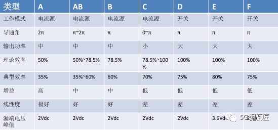
Traditional linear power amplifiers operate at very high frequencies but have a relatively narrow bandwidth. RF power amplifiers generally use selective frequency networks as load circuits. RF power amplifiers can be categorized into three classes based on the conduction angle of the current: Class A, Class B, and Class C. Class A amplifiers have a conduction angle of 360°, suitable for low-power amplification of small signals. Class B amplifiers have a conduction angle of 180°, while Class C amplifiers have a conduction angle of less than 180°. Both Class B and Class C are suitable for high-power operating states, with Class C providing the highest output power and efficiency among the three classes. RF power amplifiers mostly operate in Class C, but the current waveform distortion in Class C amplifiers is too significant, making them suitable only for use with tuned circuits as load resonant power amplifiers. Because tuned circuits have filtering capabilities, the loop current and voltage remain close to sinusoidal, resulting in minimal distortion.
Switching mode power amplifiers (SMPA) operate electronic devices in a switching state, commonly including Class D and Class E amplifiers. Class D amplifiers are more efficient than Class C amplifiers. SMPA drives active transistors into switch mode, where the transistor’s operational state is either on or off, with no overlap in voltage and current waveforms, achieving zero DC power consumption and an ideal efficiency of up to 100%.
Traditional linear power amplifiers have high gain and linearity but low efficiency, whereas switching mode power amplifiers have high efficiency and high output power but poor linearity. See the table below:
Circuit Composition
Amplifiers come in different types; simplified, the circuit of an amplifier can consist of the following parts: transistor, bias and stabilization circuits, and input-output matching circuits.
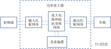
1-1. Transistor
There are many types of transistors, and various structures of transistors have been invented. Essentially, the operation of a transistor is manifested as a controlled current source or voltage source, with the working mechanism transforming unutilized DC energy into “useful” output. The DC energy is obtained from the external environment, consumed by the transistor, and converted into useful components. Different transistors have different “capabilities,” such as their power handling capabilities, which differ due to their ability to obtain DC energy; their response speeds, which determine the bandwidth they can operate within; and their input and output impedances, which affect how easily they can be matched.
1-2. Bias and Stabilization Circuits
Bias and stabilization circuits are two different circuits, but because they are often difficult to differentiate and have similar design goals, they can be discussed together.
The operation of a transistor requires certain bias conditions, known as the static operating point. This is fundamental to the transistor’s operation and its “positioning.” Each transistor has a specific positioning, and different positions will determine its operating mode, with different performance characteristics existing at various positions. Some positioning points have minimal fluctuations, suitable for small signal operations; some have larger fluctuations, suitable for high power outputs; some require less input, releasing pure energy, suitable for low noise operations; while some positioning points see the transistor oscillating between saturation and cutoff, operating in a switching state. An appropriate bias point is the foundation for normal operation. When designing broadband power amplifiers or operating at higher frequencies, the bias circuit significantly impacts circuit performance, and hence should be considered part of the matching circuit.
There are two main types of bias networks: passive and active. Passive networks (self-bias networks) typically consist of resistive networks that provide suitable operating voltage and current for the transistor. Its main drawback is that it is very sensitive to changes in transistor parameters and has poor temperature stability. Active bias networks can improve the stability of the static operating point and provide good temperature stability, but they also have issues, such as increasing circuit size, complicating circuit layout, and increasing power consumption.
The stabilization circuit must be placed before the matching circuit because the transistor needs to incorporate the stabilization circuit as part of itself before interacting with the external world. From the outside perspective, the transistor with a stabilization circuit appears as a “new” transistor. It makes certain “sacrifices” to gain stability. The mechanism of the stabilization circuit ensures that the transistor operates smoothly and steadily.
1-3. Input-Output Matching Circuits
The purpose of the matching circuit is to select a method of acceptance. For transistors that aim to provide higher gain, the approach is to accept and output comprehensively. This means that through the interface of the matching circuit, communication between different transistors is smoother, and for different types of amplifiers, the matching circuit does not only have one design method of “comprehensive acceptance.” Some small transistors with low DC and shallow roots prefer to make certain blocks during acceptance to achieve better noise performance, but blocking too much would affect their contribution. For some large power transistors, caution is needed during output because they are more unstable, and a certain retention helps them deliver more “undistorted” energy.
Typical impedance matching networks include L-matching, π-matching, and T-matching. L-matching is characterized by its simple structure and only two degrees of freedom, L and C. Once the impedance transformation ratio and resonant frequency are determined, the network’s Q value (bandwidth) is also established. One advantage of the π-matching network is that any parasitic capacitance connected to it can be absorbed into the network, leading to the widespread application of π-matching networks, as parasitic components are often dominated by capacitance in many practical situations. T-matching can be used to absorb parasitic parameters into the network when the parasitic parameters at the power supply and load ends are primarily inductive.
Ensuring Stability in RF PA Implementation
Every transistor is potentially unstable. A good stabilization circuit can integrate with the transistor to form a “sustainable operating” mode. The implementation of stabilization circuits can be classified into two types: narrowband and broadband.
Narrowband stabilization circuits consume a certain amount of gain. This stabilization circuit is realized by increasing certain consumption circuits and selective circuits. This type of circuit allows the transistor to contribute only within a very small frequency range. The other type of broadband stabilization introduces negative feedback, allowing the circuit to operate over a wide range.
The source of instability is positive feedback. The narrowband stabilization approach is to suppress a portion of the positive feedback, which also simultaneously suppresses the contribution. However, if negative feedback is done well, it can yield many additional benefits. For example, negative feedback may allow the transistor to operate without matching, enabling good interaction with the external environment. Additionally, the introduction of negative feedback enhances the linear performance of the transistor.
Techniques for Improving Efficiency in RF PA
Transistor efficiency has a theoretical limit that varies with the choice of bias point (static operating point). Additionally, poorly designed peripheral circuits can greatly reduce efficiency. Currently, engineers have limited methods to improve efficiency. Here, we will discuss two: envelope tracking technology and Doherty technology.
The essence of envelope tracking technology is to separate the input into two components: phase and envelope, and amplify them separately using different amplifier circuits. This way, the two amplifiers can focus on their respective parts, and their cooperation can achieve higher efficiency.
The essence of Doherty technology is to use two identical transistors, where only one operates at low input and remains in an efficient state. If the input increases, both transistors operate simultaneously. This method relies on the coordination between the two transistors. The operational state of one transistor directly determines the efficiency of the other.
Testing Challenges Faced by RF PA
Power amplifiers are critical components in wireless communication systems, but they are inherently nonlinear, leading to spectral regrowth that can interfere with adjacent channels and potentially violate mandated out-of-band radiation standards. This characteristic can even cause in-band distortion, increasing the bit error rate (BER) and reducing data transmission rates.
Under the peak-to-average power ratio (PAPR), the new OFDM transmission format may have more sporadic peak power, making it difficult for the PA to be segmented. This will reduce spectral mask compliance and increase the overall waveform’s EVM and BER. To address this issue, design engineers often deliberately reduce the operational power of the PA. Unfortunately, this is an inefficient method since reducing the operational power of the PA by 10% can lead to a 90% loss in DC power.
Currently, most RF PAs support multiple modes, frequency ranges, and modulation modes, making the testing requirements more extensive. Thousands of test items are not uncommon. The application of new technologies such as Crest Factor Reduction (CFR), Digital Predistortion (DPD), and Envelope Tracking (ET) helps optimize PA performance and power efficiency, but these technologies complicate testing and significantly extend design and testing times. Increasing the bandwidth of RF PAs will lead to a fivefold increase in the bandwidth required for DPD measurements (possibly exceeding 1 GHz), further complicating testing.
Trends indicate that to increase efficiency, RF PA components and front-end modules (FEM) will be more tightly integrated, and a single FEM will support a wider range of frequency bands and modulation modes. Integrating envelope tracking power supplies or modulators into FEM can effectively reduce the overall space requirements within mobile devices. However, significantly increasing the number of filter/duplexer slots to support a broader operational frequency range will increase the complexity of mobile devices and the number of testing items.
Changes in Semiconductor Materials:
Ge (Germanium), Si (Silicon) →→→ GaAs (Gallium Arsenide), InP (Indium Phosphide) →→→ SiC (Silicon Carbide), GaN (Gallium Nitride), SiGe (Silicon Germanium), SOI (Silicon on Insulator) →→→ Carbon Nanotubes (CNT) →→→ Graphene.
Currently, the mainstream process for power amplifiers is still the GaAs process. Additionally, GaAs HBT, or Heterojunction Bipolar Transistor, is a type of bipolar transistor composed of GaAs layers and AlGaAs layers.
Although CMOS technology has matured, the application of Si CMOS power amplifiers is not widespread. In terms of cost, although silicon wafers from CMOS technology are cheaper, the layout area of CMOS power amplifiers is relatively large, and the high R&D costs associated with the complex design of CMOS PAs diminish the overall cost advantage.
Carbon Nanotubes (CNT), due to their small physical size, high electron mobility, high current density, and low intrinsic capacitance, are considered ideal materials for nanoelectronic devices.
Zero bandgap semiconductor material Graphene, due to its high electron mobility, nanoscale physical size, excellent electrical properties, and mechanical properties, is expected to become a popular material for the next generation of RF chips.
Linearization Techniques for RF PA
Nonlinear distortion in RF power amplifiers can generate new frequency components, such as second-order distortion producing second harmonics and intermodulation, while third-order distortion produces third harmonics and multiple tones. If these new frequency components fall within the passband, they will directly interfere with the transmitted signal; if they fall outside the passband, they will interfere with signals from other channels. Therefore, linearization processing of RF power amplifiers is necessary to better resolve the signal spectrum regeneration issue.
The basic principles and methods of RF amplifier linearization technology revolve around using the amplitude and phase of the input RF signal envelope as a reference, comparing it with the output signal, and subsequently generating appropriate corrections. Currently, widely applied linearization techniques for power amplifiers include power back-off, negative feedback, feedforward, predistortion, envelope elimination and restoration (EER), and linear amplification using nonlinear components (LINC). More complex linearization techniques, such as feedforward, predistortion, and envelope elimination and restoration, show better improvement in amplifier linearity. In contrast, simpler linearization techniques like power back-off and negative feedback provide limited improvement in linearity.
2-1. Power Back-Off
This is the most common method, which involves using a larger power transistor as a small power transistor, effectively sacrificing DC power consumption to improve amplifier linearity.
The power back-off method involves reducing the input power of the power amplifier from the 1dB compression point (the amplifier has a linear dynamic range, within which the output power increases linearly with input power. As the input power continues to increase, the amplifier gradually enters saturation, and power gain begins to decline, with the output power defined as the 1dB compression point when the gain drops below linear gain) backward by 6-10 decibels, operating at levels far below the 1dB compression point to keep the power amplifier away from saturation and in the linear operating region, thereby improving the third-order intermodulation coefficient of the power amplifier. Generally, when the fundamental power is reduced by 1dB, the third-order intermodulation distortion improves by 2dB.
Power back-off is simple and easy to implement, requiring no additional equipment, making it an effective method to improve amplifier linearity. However, it significantly reduces efficiency. Moreover, when power back-off reaches a certain point, and the third-order intermodulation reaches below -50dBc, further back-off will no longer improve the amplifier’s linearity. Therefore, in situations requiring high linearity, relying solely on power back-off is insufficient.
2-2. Predistortion
Predistortion involves adding a nonlinear circuit before the power amplifier to compensate for the nonlinear distortion of the power amplifier.
The advantage of predistortion linearization technology is that it does not have stability issues, has a wider signal bandwidth, and can handle multi-carrier signals. Predistortion technology is cost-effective, consisting of several carefully selected components packaged into a single module, connected between the signal source and the power amplifier, creating a predistortion linear power amplifier. The power amplifiers in handheld mobile stations have adopted predistortion technology, reducing intermodulation products by several dB with only a few components, which is a critical few dB.
Predistortion technology can be divided into two basic types: RF predistortion and digital baseband predistortion. RF predistortion generally uses analog circuits, offering advantages such as simple circuit structure, low cost, and suitability for high-frequency, broadband applications, but it has the drawback of limited improvement in spectral regeneration components and difficulty in canceling high-order spectral components.
Digital baseband predistortion can be implemented using digital circuits due to its low operating frequency, offering strong adaptability and the ability to counteract high-order intermodulation distortion by increasing sampling frequency and quantization levels. This method has promising development potential. This predistortion device consists of a vector gain controller that adjusts the amplitude and phase of the input signal based on the contents of a lookup table (LUT), with the size of the predistortion controlled by the LUT input. Once optimized, the vector gain controller provides a nonlinear characteristic opposite to that of the power amplifier. Ideally, the output intermodulation products should equal the output amplitude of the dual-tone signal through the power amplifier, with opposite phases, meaning the adaptive adjustment module aims to minimize the difference between the input signal and the power amplifier output signal. Note that the envelope of the input signal is also an input to the lookup table, with a feedback path sampling the distortion output of the power amplifier, which is then converted to A/D and sent to the adaptive adjustment DSP to update the lookup table.
2-3. Feedforward
Feedforward technology originates from “feedback” and is not a new technology, having been proposed by Bell Labs in the 1920s and 1930s. Conceptually, apart from calibration (feedback) applied to the output, it is entirely “feedback”.
Feedforward linear amplifiers consist of two loops connected through couplers, attenuators, synthesizers, delay lines, and power splitters. After the RF signal input, the power splitter divides it into two paths. One path goes into the main power amplifier, which, due to its nonlinear distortion, outputs not only the main frequency signal that needs amplification but also third-order intermodulation interference. A portion of the signal is coupled from the output of the main amplifier, through loop 1, to cancel the main carrier frequency signal, leaving only the inverted third-order intermodulation component. The third-order intermodulation component is amplified by the auxiliary amplifier and then goes through loop 2 to cancel the intermodulation components generated by the nonlinearity of the main amplifier, thereby improving the linearity of the amplifier.
Feedforward technology provides high calibration precision without the drawbacks of instability and bandwidth limitations. However, these advantages come at a high cost, as the output calibration requires the calibration signal to be amplified to high power levels, necessitating additional auxiliary amplifiers, which must have distortion characteristics that exceed the specifications of the feedforward system.
The cancellation requirements for feedforward amplifiers are stringent, requiring matching in amplitude, phase, and delay. Variations in power, temperature, and device aging can all cause cancellation failure. Therefore, adaptive cancellation techniques should be considered in the system to ensure that cancellation can keep up with internal and external environmental changes.
Industry Chain Situation of RF Power Amplifiers
1. Major Opportunities for RF PA in 5G Smart Mobile Terminals
1. The Crown Jewel of RF Devices
RF power amplifiers (PA) are the main components of the RF front-end transmission path, primarily used to amplify the small power RF signals generated by modulation oscillator circuits to obtain sufficiently large RF output power for transmission to antennas. They are typically used to amplify RF signals in the transmission channel.
Mobile RF front-ends: Once connected to a mobile network, any smartphone can easily browse social media, watch HD videos, download images, and shop online, all thanks to the evolution of RF front-ends. Each network standard (2G/3G/4G/WiFi/GPS) requires its own RF front-end module, serving as the bridge for communication between the phone and the outside world—the more features a phone has, the greater its value.
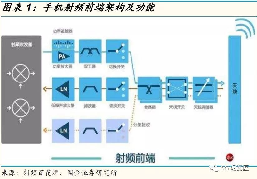
The RF front-end module is a core component of mobile terminal communication systems. Its importance can be considered from two aspects: necessity, as it is the essential link between the communication transceiver and the antenna; and importance, as its performance directly determines the communication modes supported by the mobile terminal, as well as key performance indicators like signal strength, call stability, and transmission power, directly affecting user experience.
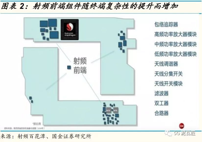
RF front-end chips include power amplifiers (PA), antenna switches (Switch), filters (Filter), duplexers (Duplexer and Diplexer), and low-noise amplifiers (LNA), playing a core role in multi-mode/multi-frequency terminals.
The largest market in the RF front-end industry is filters, which are expected to grow from $8 billion in 2017 to $22.5 billion by 2023, with a compound annual growth rate of 19%. This growth is primarily driven by the significant increase in the penetration of BAW filters, with typical applications such as the ultra-high frequency bands defined by 5G NR and WiFi diversity antenna sharing.
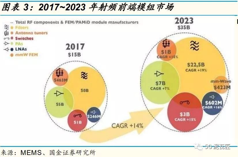
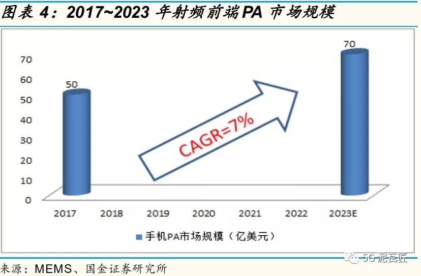
The power amplifier market is relatively stable, with a compound annual growth rate of 7%, expected to grow from $5 billion in 2017 to $7 billion by 2023. The growth of high-end LTE power amplifiers, especially in high and ultra-high frequencies, will compensate for the decline in 2G/3G markets.
2. 5G Drives Simultaneous Growth in Volume and Price of Mobile RF PAs
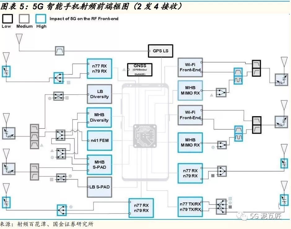
The RF front-end evolves alongside smart terminals. In the 4G era, smartphones generally adopted a 1 transmit 2 receive architecture. With 5G introducing new frequency bands (n41 2.6GHz, n77 3.5GHz, and n79 4.8GHz), the RF front-end of 5G smartphones will undergo new changes, while also considering that 5G smartphones will continue to be compatible with 4G, 3G, and 2G standards, making the RF front-end of 5G smartphones exceptionally complex.
It is predicted that in the 5G era, smartphones will adopt a 2 transmit 4 receive scheme.
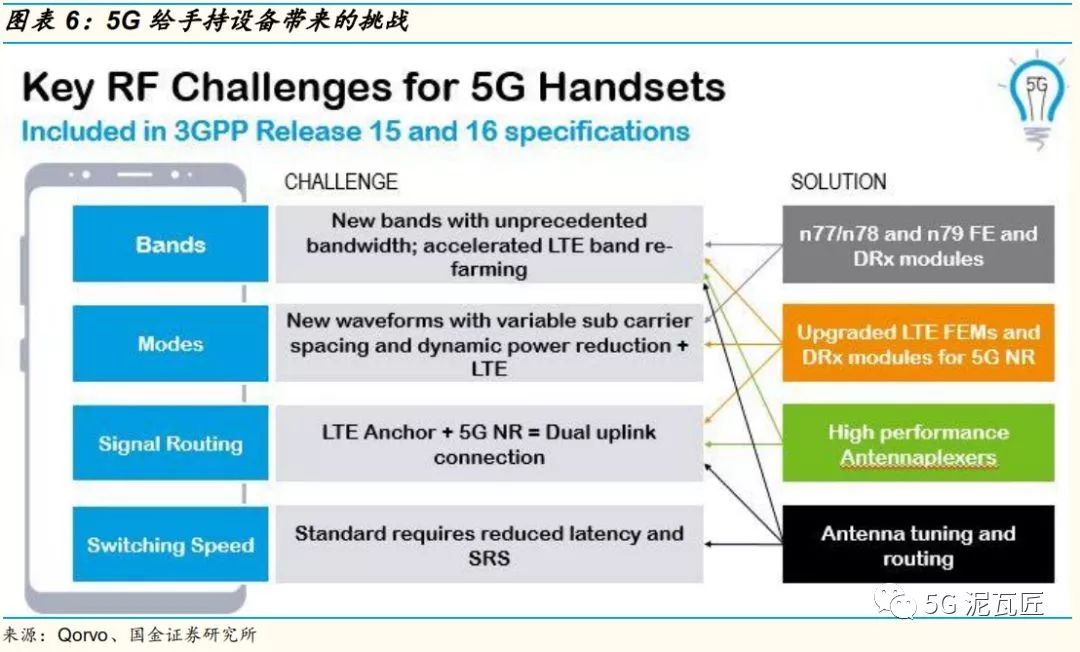
In both base stations and device terminals, the challenges brought by 5G to suppliers primarily manifest in the RF domain, as this is the critical entry point for devices to connect to the internet. The upcoming 5G smartphones will face multiple challenges:
Support for more frequency bands: As the familiar b41 transforms into n41, n77, and n78, support for more frequency bands will be required;
Different modulation directions: As 5G focuses on high-speed connections, there will be new changes in modulation, with more stringent power consumption requirements. For example, in the 4G era, the focus was on ACPR. In the 5G era, the emphasis will shift to EVM (generally less than 1.5%);
Signal routing choices: Choosing between 4G anchor + 5G data connection or directly using 5G will bring different challenges.
Changes in switching speed: Although there may not be significant changes in this aspect, SRS will also bring new challenges.
Other new frequency bands such as n77/n78/n79 will also impact the RF front-end’s form, driving changes in front-end modules to meet the requirements of new frequency bands and tuning methods.
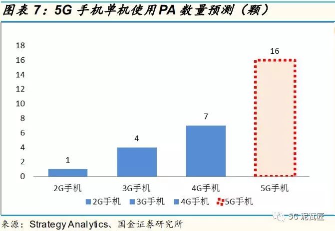
The usage of power amplifiers (PA) in 5G smartphones is expected to double: PA is one of the most critical components in a smartphone, directly determining the wireless communication distance, signal quality, and even standby time, making it the most important part of the entire RF system aside from the baseband. The number of PAs in smartphones has gradually increased with the transition from 2G, 3G, 4G, to 5G. For example, a multi-mode multi-frequency 4G smartphone requires 5-7 PA chips, while it is predicted that 5G smartphones will contain as many as 16 PA chips.
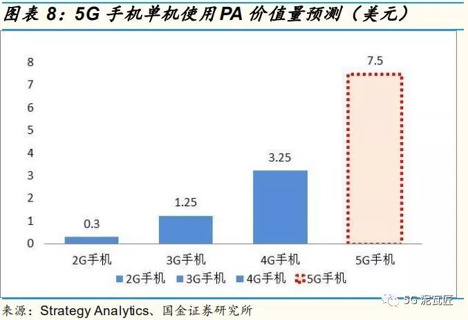
The single-unit value of power amplifiers (PA) in 5G smartphones is expected to reach $7.5: Simultaneously, the unit price of PAs has also significantly increased, with the average unit price of PA in 2G smartphones being $0.3, rising to $1.25 for 3G smartphones, and reaching $3.25 for multi-mode 4G smartphones. It is expected that the value of 5G smartphone PAs will exceed $7.5.
3. GaAs RF Devices Will Continue to Dominate the Mobile Market
In the 5G era, GaAs materials are suitable for mobile terminals. The electron mobility of GaAs is six times that of Si, with a direct bandgap, making its devices relatively high-frequency and high-speed compared to Si devices, which are recognized as suitable semiconductor materials for communication. Currently, the majority of RF power amplifiers in mobile wireless communication applications use GaAs materials. In GSM communication, domestic chip design companies like Ruideke and Hantex have leveraged the high integration and low-cost advantages of RF CMOS processes to break the dominance of traditional GaAs processes used by international leading manufacturers in RF power amplifiers.
However, in the 4G era, due to the high-frequency losses, high noise, and low output power density of Si materials, RF CMOS no longer meets the requirements, and mobile RF power amplifiers have returned to the era dominated by GaAs processes. Unlike RF power amplifier devices that rely on GaAs materials, 90% of RF switches have shifted from traditional GaAs processes to SOI (Silicon on Insulator) processes, and most RF transceivers have also adopted RF CMOS processes to meet the increasing demand for integration.
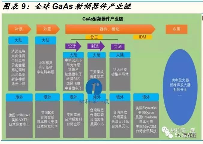
In the 5G era, GaN materials are suitable for base stations. In macro base station applications, GaN materials are gradually replacing Si LDMOS due to their high frequency and high output power advantages. In micro base stations, GaAs PAs will still dominate for the time being due to their market-validated reliability and cost-effectiveness. However, as device costs decrease and technology improves, GaN PAs are expected to gain a share in micro base station applications. In mobile terminals, due to high costs and high power supply voltage, GaN PAs cannot shake the dominance of GaAs PAs in the short term.
2. 5G Base Stations Will See Significant Growth in PA Demand, GaN Has Great Potential
1. Significant Increase in RF PA Demand for 5G Base Stations
The number of PAs in 5G base stations is expected to increase 16-fold. 4G base stations use a 4T4R scheme, with a corresponding demand for 12 PAs across three sectors. For 5G base stations, the expected 64T64R will become the mainstream scheme, with a demand for as many as 192 PAs, leading to a significant increase in PA numbers.
RF PAs for 5G base stations are expected to see simultaneous growth in volume and price. Currently, the primary power amplifier technology for base stations is based on silicon lateral diffusion metal-oxide-semiconductor (LDMOS), but LDMOS technology is only suitable for low-frequency bands and has limitations in high-frequency applications. Some requirements for 5G base station PAs may include operating frequencies of 3~6GHz and 24GHz~40GHz, with RF power ranging from 0.2W to 30W. GaN RF PAs are expected to gradually become the dominant technology, although GaN is priced higher than LDMOS and GaAs.
GaN has excellent high power density and high frequency characteristics. The simplest way to increase RF power in power amplifiers is to increase the voltage, making GaN transistor technology very attractive. Comparing different semiconductor process technologies reveals how power typically increases with high operating voltage IC technology.
The typical processing steps for GaN RF devices mainly include: epitaxial growth, device isolation, ohmic contact (fabricating source and drain), nitride passivation, gate fabrication, field plate fabrication, substrate thinning, and substrate via holes.
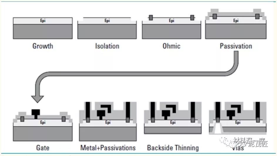
Processing Steps for GaN RF Devices
2. GaN RF PAs are Expected to Become the Mainstream Technology for 5G Base Stations
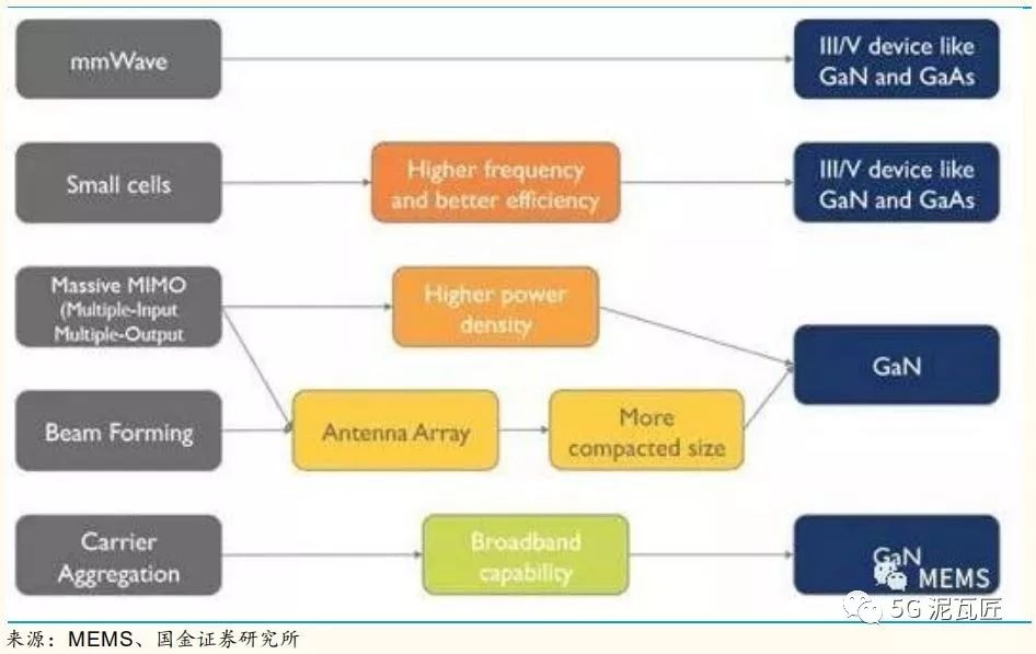
It is predicted that most applications below 6GHz in macro network units will adopt GaN devices, while GaAs will have more advantages in small base stations. In the telecom market, the imminent arrival of 5G network applications will bring enormous market opportunities for GaN devices starting from 2019. Compared to existing silicon LDMOS (laterally diffused metal-oxide-semiconductor technology) and GaAs (gallium arsenide) solutions, GaN devices can provide the power and performance needed for the next generation of high-frequency telecom networks. Moreover, the broadband performance of GaN is also a key factor for implementing important new technologies such as multi-band carrier aggregation. GaN HEMT (High Electron Mobility Transistor) has become a candidate technology for future macro base station power amplifiers.
Since LDMOS can no longer support higher frequencies and GaAs is no longer the optimal solution for high-power applications, it is expected that most applications below 6GHz in macro network units will adopt GaN devices. The higher frequency used in 5G networks results in poorer penetration and coverage compared to 4G, which means that small cells will play a significant role in 5G network construction. However, since small cells do not require such high power, existing technologies like GaAs still have their advantages. At the same time, because higher frequencies reduce the coverage of each base station, more transistors will be needed, and the market shipment growth rate is expected to accelerate.
Main Trends in Base Stations from 2015 to 2025
3. Global Competitive Landscape of GaN RF Device Industry Chain
The launch speed of GaN microwave RF device products has significantly accelerated. Currently, although the microwave RF field is attracting attention, due to high technical levels and significant patent barriers, there are relatively few companies in this field compared to the power electronics and optoelectronics sectors, but most have strong research capabilities and market operation abilities. The commercialization of GaN microwave RF devices has rapidly developed. According to Material Deep’s statistical analysis of Mouser data, as of April 2018, four manufacturers have launched 150 categories of GaN HEMT, accounting for 9.9% of the entire RF transistor supply categories, a 0.6% increase from January.
Qorvo products have the widest operating frequency range, while Skyworks products have a smaller range. Qorvo, CREE, and MACOM have 73% of their products’ output power concentrated between 10W and 100W, with maximum power reaching 1500W (operating frequency at 1.0-1.1GHz, produced by Qorvo), primarily using the GaN/SiC GaN route. Additionally, some companies offer GaN RF module products, with four companies providing sales of GaN RF amplifiers, of which Qorvo has the widest operating frequency range, with a maximum frequency of up to 31GHz. Skyworks products have a smaller operating frequency range, primarily concentrated between 0.05-1.218GHz.
Qorvo has the most product categories in RF amplifiers. Among the two 5G working frequency bands (3.3-3.6GHz and 4.8-5GHz) announced by China’s Ministry of Industry and Information Technology, Qorvo has the most product categories, with maximum powers of 100W and 80W, respectively (in January, Qorvo’s product at 4.8-5GHz had a maximum power of 60W), while ADI’s maximum power at 4.8-5GHz increased to 50W (previously below 40W), with most other products below 50W.
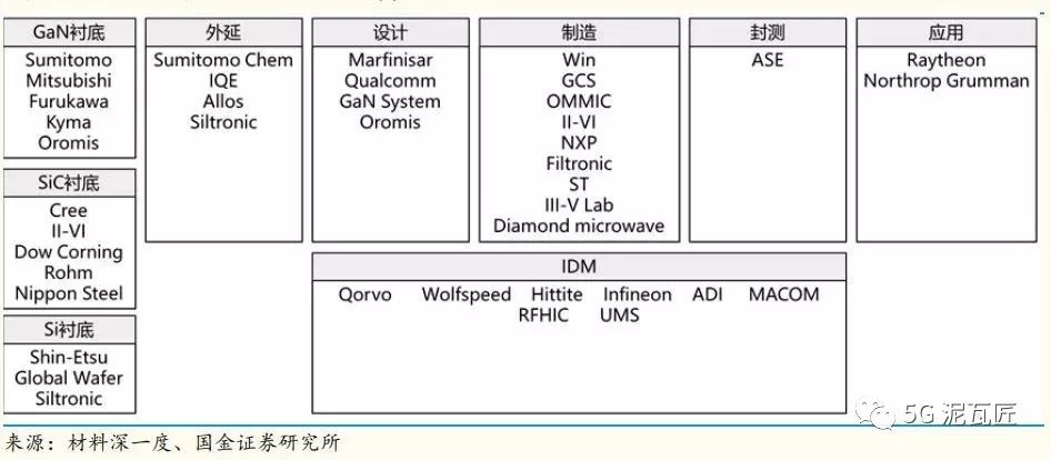
Key Companies in the Global GaN RF Device Industry Chain
Finally, the report lists some key beneficiary companies in the RF power amplifier industry chain.
Base station RF PA: Qorvo, CREE, Wenmao, Xuanji Information (proposed acquisition of Anpulon), Sanan Optoelectronics, Hi-Tech High New (Haiwei Huaxin);
Mobile terminal and IoT RF PA: Skyworks, Qorvo, Qualcomm, Taiwan Wenmao, Sanan Optoelectronics, Huaxin Electronics, Zhuosheng Microelectronics, Xinwei Communication.