Source: Old Tiger Talks Chips
Original Author: Old Tiger Talks Chips
This article briefly introduces the concept, technology, processes, and future development trends of Multi-Chip Packaging.
Multi-Chip Packaging technology (MCP) is a key technology in the field of modern integrated circuits (IC), used to integrate multiple chips or functional units within a single package. This technology significantly enhances device performance, bandwidth, and energy efficiency through spatial optimization and functional synergy, making it a core foundation for future high-performance computing, artificial intelligence, and communication fields.
1. Basic Concept of Multi-Chip Packaging
1.1 Definition and Core Idea
Multi-Chip Packaging is a technology that integrates multiple chips (logic chips, memory chips, RF chips, etc.) into a single package. It includes 2.5D packaging (connected via silicon interposer) and 3D packaging (vertically stacked chips), achieving higher integration and performance.
Analogy: Multi-Chip Packaging can be understood as building a “micro-city”: each chip is a functional area, connected by “roads” (interconnection structures) to achieve efficient collaboration.
Performance Improvement: Shortens signal transmission paths between chips, reducing latency and power consumption.
Space Saving: Smaller package size is suitable for mobile devices and high-density servers.
Modular Design: Facilitates flexible combinations of different functional chips, reducing design complexity.
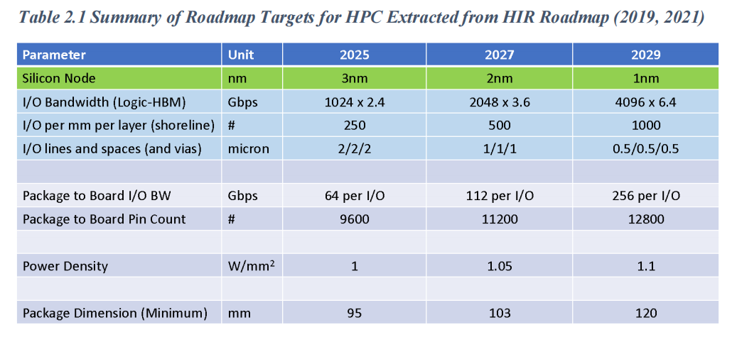
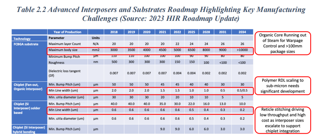
Advanced substrates are the physical carriers of Multi-Chip Packaging, and their performance directly determines the speed and power consumption of signal transmission. Current technology requires the line width/spacing of advanced substrates to be at 1/1μm or even smaller to meet high bandwidth and low power consumption requirements.
Current Gap: The U.S. supply chain lags behind Asia in advanced substrate manufacturing, especially in fine pitch redistribution layer (RDL) technology.
Future Goal: HIR plans to achieve 0.5/0.5μm line width/spacing by 2030.
2.2 Interconnection Technology
Inter-chip interconnection is the core challenge of Multi-Chip Packaging. The two main technologies include:
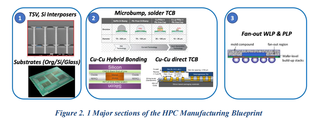
Silicon Interposer: Provides high-density interconnection, supporting greater bandwidth, but has high manufacturing costs.
Organic Substrates: Lower cost, but with slightly inferior signal integrity and heat dissipation performance.
The increase in package power density poses higher requirements for thermal management.
Challenge: A thermal design power (TDP) of 200-400W requires effective heat dissipation solutions.
Solutions: Introduce advanced thermal conductive materials within the package, integrated thermal interface materials (TIM), and liquid cooling technologies.
The high bandwidth demand makes power delivery a significant bottleneck.
Issue: Traditional discrete power components can no longer meet the high power density requirements within the package.
Solution: Technology based on integrated voltage regulators (IVR) within the package, utilizing inductance and switched capacitance for efficient power delivery.
3.1 Manufacturing Processes
The realization of Multi-Chip Packaging relies on high-precision manufacturing processes, mainly including:
Fine pitch RDL manufacturing: Current investments are mainly concentrated in Asia, requiring breakthroughs to achieve higher line width/spacing.
Panel Level Packaging (PLP): Provides a more cost-effective solution for large-size packages.
Multi-Chip Packaging requires support from new materials:
Interposer replacement materials: Such as high-density ceramic substrates, which have higher thermal conductivity and mechanical strength.
Packaging materials: Need to support higher thermal conductivity and lower resistance.
The mechanical stress and thermal expansion mismatch caused by stacked chips and fine pitch interconnections need to be addressed to ensure long-term reliability of the package.
4. Future Development Trends
4.1 Chiplet and Heterogeneous Integration
Chiplet technology integrates chips from different process nodes and functional modules. Compared to traditional monolithic designs, chiplets offer greater flexibility and performance.
HBM3 Applications: For example, high bandwidth memory (HBM3) requires a data rate of 4-6Gbps per channel, with the number of I/Os in the package rapidly increasing, and the number of HBM per silicon node will increase by 1.4 times.
4.2 Expansion of 2.5D and 3D Packaging
2.5D Packaging: Extends EMIB technology to increase bandwidth density and reduce costs.
3D Packaging: Achieves higher performance density through vertical stacking, but poses higher requirements for thermal management and manufacturing precision.
4.3 High-Density Substrate Technology
The future goal is to improve the performance of organic substrates and panel-level substrates to below 1/1μm, achieving lower resistance and higher transmission speeds.
Power integration technology within the package will be further optimized, supporting high power applications through localized voltage regulators and efficient power delivery components.
Multi-Chip Packaging technology has become a key direction in the integrated circuit industry, with advantages in performance enhancement, space saving, and support for diverse applications. However, this technology still faces challenges in substrate manufacturing, thermal management, and power delivery, requiring continuous innovation from multiple dimensions including materials, processes, and design.
END
Reproduced content only represents the author’s views
Does not represent the position of the Institute of Semiconductors, Chinese Academy of Sciences
Editor: Schrödinger’s Cat
Responsible Editor: Six Dollar Fish
Submission Email: [email protected]
1. The Semiconductor Institute has made progress in the research of bionic covering neuron models and learning methods
2. The Semiconductor Institute has made significant progress in inverted structure perovskite solar cells
3. Why is copper used as the interconnect metal in chips?
4. What exactly is the 7nm in chips?
5. Silicon-based integrated optical quantum chip technology
6. How anomalous is the quantum anomalous Hall effect? It may lead to the next information technology revolution!