K sodium niobate(KNN)-based lead-free piezoelectric ceramics have become one of the most promising alternatives to lead-based piezoelectric ceramics due to their excellent piezoelectric properties, high Curie temperature, and simple preparation process. Piezoelectric ceramic devices such as ultrasonic transducers need to withstand large mechanical loads during operation, which can easily lead to microcracks and fracture failure over prolonged periods of mechanical load. Therefore, research on the mechanical properties of piezoelectric ceramics is of great significance for the long-term stable and safe operation of piezoelectric devices.
Recently, a research team from the School of Materials Science and Engineering at Hubei University conducted a comprehensive study on the mechanical and electrical properties of KNN-based piezoelectric ceramics and lead zirconate titanate(PZT)-based piezoelectric ceramics. They found that, compared to PZT-based piezoelectric ceramics, KNN-based piezoelectric ceramics doped with metal oxides exhibited not only excellent electrical properties but also superior mechanical properties due to their highly dense structure and the presence of nanoscale amorphous layers at the grain boundaries. The Young’s modulus of the prepared KNN-based piezoelectric ceramics was E = 88.81 – 98.37 GPa, nanoindentation hardness H = 5.40 – 7.89 GPa, fracture toughness KIC = 1.520 – 1.974 MPa·m1/2, and bending strength σf = 160.68 – 235.78 MPa. In contrast, the Young’s modulus of PZT-based piezoelectric ceramics was E = 65 – 85 GPa, nanoindentation hardness H = 3.91 GPa, fracture toughness KIC = 1.242 – 1.446 MPa·m1/2, and bending strength σf = 60 – 80 MPa. This article, titled “Achieving excellent mechanical and electrical properties in transition metal oxides and rare earth oxides-doped KNN-based piezoceramics”, was published in the ceramics journal Journal of the American Ceramic Society and was recommended as an “Editor’s Choice” article by the editor.
Nanoindentation technology can quantitatively characterize the intrinsic mechanical properties of materials in the submicron to several tens of microns range, and it is widely used in the study of metallic materials. By varying stress levels, loading rates, and load holding times, information about material hardness, fracture toughness, creep, and dislocation nucleation and activation can be extracted. Recent research has introduced this technology into the study of ceramic materials. Nanoindentation technology has unique advantages over traditional macroscopic mechanical measurement methods:(a) Its load range is 1 – 50 mN, and the indentation size is between submicron to several tens of microns. The grain size of KNN-based ceramics is typically around 2 – 3 μm, allowing for appropriate loads to be applied to the grain or grain boundary regions to quantitatively study the mechanical properties of different areas. Conventional Vickers hardness or three-point bending test methods use large-sized samples and are considered macroscopic testing methods. Their results are significantly affected by porosity, surface cracks introduced during polishing, and sample geometry, making them more suitable for engineering evaluations of material macro-properties. Nanoindentation technology can collect hundreds to thousands of data points in a smaller area at once and can filter out invalid data caused by factors such as porosity and secondary phases using optical or electron microscopy. Therefore, nanoindentation technology can obtain the intrinsic mechanical properties of materials.KNN-based ceramics generally exhibit tetragonal grains with an average size of 2 – 3 μm, and the large number of data points also eliminates the influence of grain orientation on mechanical properties that may arise from the polycrystalline structure of ceramics. Based on experimental results, no significant data variation caused by the polycrystalline structure was observed for KNN-based ceramics.
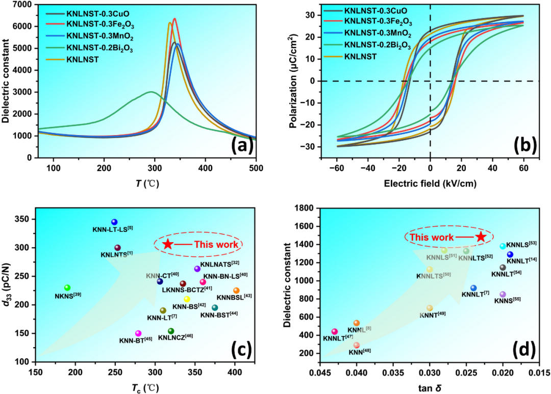
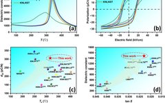
Figure 1Electrical properties of a series of prepared KNN-based piezoelectric ceramics.
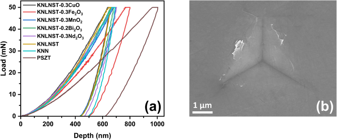
Figure 2 (a) Nanoindentation load-displacement curves of PSZT and KNN-based piezoelectric ceramics; (b) SEM image of the Berkovich indentation on the ceramic surface.
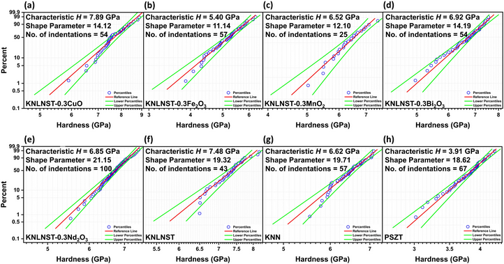
Figure 3 Weibull distribution of nanoindentation hardness for PSZT and KNN-based piezoelectric ceramics.
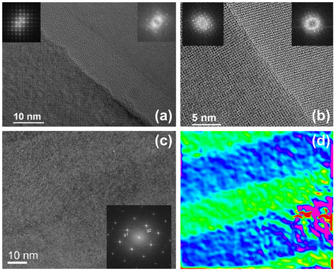
Figure 4 (a, b) HRTEM images of KNNL NST + 0.05 mol% Fe2O3 + 0.015 mol% Nd2O3 and KNNL NST; (c, d) HRTEM images, electron diffraction patterns, and GPA analysis of KNNL NST + 0.05 mol% Fe2O3 + 0.015 mol% Nd2O3.
Professors Guo Jinming and He Yunbin from the School of Materials Science and Engineering at Hubei University are the corresponding authors of this paper, with master’s student Zhang Zhidong as the first author. Collaborators include Prof. Shang Xunzhong from Hubei University, Dr. Liu Xiong from Carl Zeiss AG, and Prof. Zhang Zaoli from the Erich Schmid Institute of the Austrian Academy of Sciences.This work was supported by the National Natural Science Foundation of China.
Paper link:
https://doi.org/10.1111/jace.19865
(Click the lower left corner “Read Original” to access the original text directly)
Source: Author’s team, thanks for the strong support to this public account!
The author authorized the publication and marked it as “original”; please indicate the source when reprinting: Research and Exploration
For submissions, reprints, and collaborations, please contact WeChat: MatResFron001
Welcome to leave a message and share your views.Support the author by clicking the “like” button in the lower right corner and “view”↓↓↓