
Chasing 5G, GaAs/GaN Remains the Absolute Star. Due to the higher frequency bands and larger bandwidths of 5G solutions compared to 4G, the path loss is relatively greater, which poses new requirements for the material performance of RF front-end devices: 1) larger bandgap; 2) higher critical breakdown electric field; 3) higher thermal conductivity; 4) higher saturation electron velocity and electron mobility.
From the perspective of substrate materials, the 5G era (Sub-6GHz) is still the main battlefield for GaAs, but as it develops into higher frequency millimeter-wave stages in the medium to long term, GaAs has lower thermal conductivity and poorer heat dissipation, resulting in RF devices that can withstand relatively low power, which will likely require materials with GaN as the working layer.
Currently, GaN can be grown as epitaxial material on substrates like SiC and Si, and it is expected that GaN-on-SiC will become the mainstream semiconductor material for RF devices in macro base stations with higher power requirements in the 5G era, while GaAs will dominate in micro base stations where power consumption requirements are relatively low.
National Alliance
Smart Chip Research Report
1. Introduction to GaAs/GaN Materials
1.1、GaAs
Gallium Arsenide (GaAs) is currently one of the most important and technologically mature compound semiconductor materials. GaAs materials possess characteristics of a large bandgap and high electron mobility, and as a direct bandgap material, it has high luminous efficiency, making it the primary material used in the optoelectronics field, as well as an important microelectronic material. Based on differences in conductivity, GaAs materials can be divided into semi-insulating (SI) GaAs and semiconductor (SC) GaAs.
-
Semi-insulating GaAs wafers have the substrate insulated from the epitaxial transistor devices formed on top and are mainly used for making RF circuits.
-
Semiconductor GaAs is produced by adding molten conductive dopants to GaAs to create semi-conductive ingots, mainly used for making optoelectronic devices such as LEDs, lasers, and photovoltaic devices.
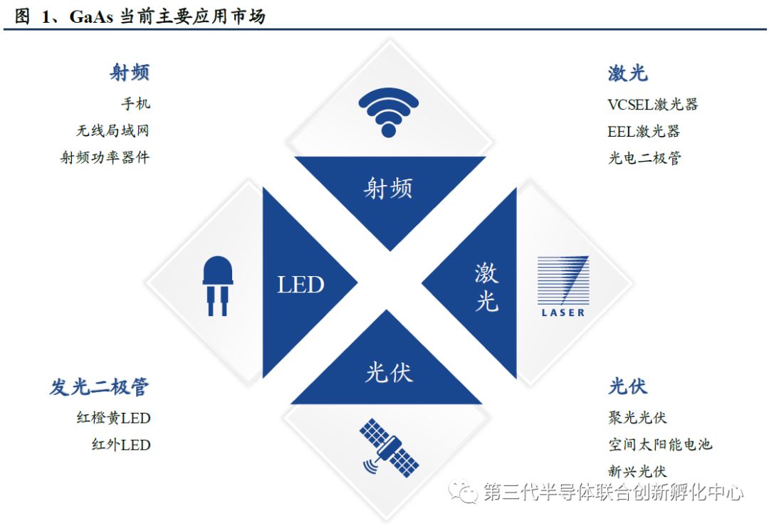
RF is currently the main downstream application of GaAs materials.
-
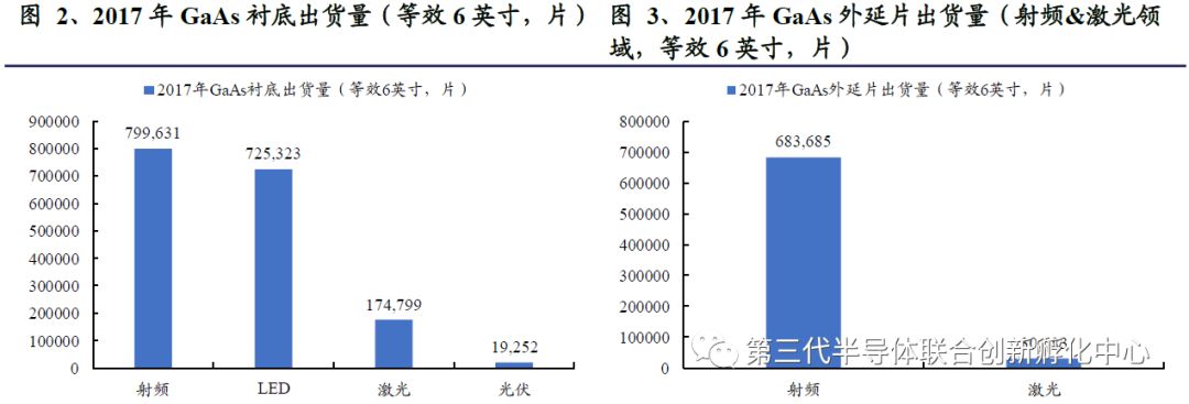
From the shipment data of GaAs substrates in 2017, among the four major application fields, RF, LEDs, lasers, and photovoltaics accounted for 46.52%, 42.19%, 10.17%, and 1.12%, respectively, with RF and LEDs being the primary markets for GaAs substrates.
-
In the epitaxial wafer field, RF and laser applications are two important markets for outsourced epitaxial wafers. According to the shipment data of GaAs epitaxial wafers in 2017, RF applications also have a significant advantage in scale.
1.2 GaN
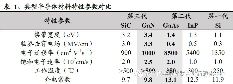
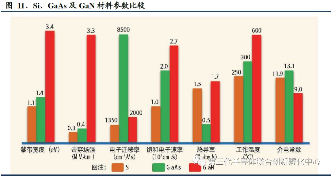
Gallium Nitride (GaN), as a typical representative of third-generation semiconductor materials, has a wider bandgap compared to the first two generations of semiconductor materials, a higher critical breakdown electric field, greater saturation electron velocity, and a smaller dielectric constant, enabling it to withstand higher operating voltages, suitable for higher frequencies, and achieve higher power densities. It also has excellent properties such as high temperature resistance, corrosion resistance, and radiation resistance, which can break through the performance limits of second-generation semiconductor materials (GaAs, InP, etc.) in multiple aspects.
Thanks to the qualitative leap in performance compared to first and second-generation semiconductor materials, GaN has become the ideal material for manufacturing short-wavelength light-emitting devices, optoelectronic detectors, and high-temperature, high-frequency, high-power electronic devices.
-
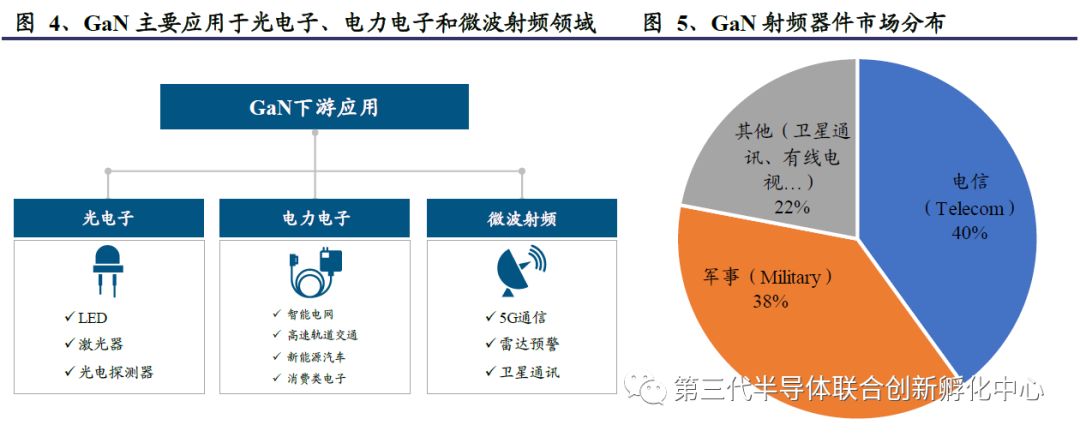
In the optoelectronics field: including short-wavelength LEDs, lasers, optoelectronic detectors, etc., especially GaN-based ultraviolet optoelectronic detectors, which can be applied in military, aerospace, environmental protection, scientific research, and other fields.
-
In the power electronics field: including controllers in smart grids, solar power generation, and wind power, the energy-saving and lossless handling of high-voltage operations also makes GaN one of the important materials for electronic devices in new energy vehicles, with low loss, high frequency, and high efficiency advantages.
-
In the microwave RF field: including 5G communication, satellite communication, radar warning (an important application scenario for GaN in the military field), GaN has advantages such as high bandwidth, high efficiency, and high power density.
Currently, GaN applications are still dominated by military uses and have begun to gradually expand into civilian fields such as automotive autonomous driving and wireless communication base stations.
With the wave of 5G, the RF industry for mobile devices is expected to usher in significant development opportunities. As an important cornerstone of devices, the demand for upstream materials is also expected to experience a new round of rapid growth.
2. Chasing 5G, GaAs/GaN Remains the Absolute Star
2.1 What New Requirements Does 5G Pose for RF Materials?
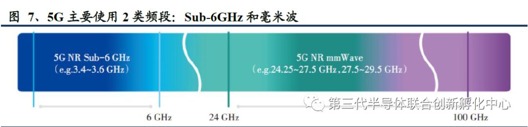
According to the 3GPP standard definition, 5G NR (New Radio) mainly uses two frequency ranges:
-
FR1 corresponds to the frequency range of 450MHz-6GHz, with a maximum channel bandwidth of 100MHz, also known as the Sub-6GHz band.
-
FR2 corresponds to the frequency range of 24.25GHz-52.60GHz, with a maximum channel bandwidth of 400MHz, which we refer to as the millimeter-wave band (mmWave).
As the frequency increases, RF materials also face new challenges. Because the frequency bands of 5G solutions are higher and the bandwidths larger than the currently mainstream 4G bands, path loss is relatively greater, which poses new requirements for the materials and processes of RF front-end devices:
1) larger bandgap to operate at higher frequency bands;
2) higher critical breakdown electric field to meet higher power applications;
3) higher thermal conductivity to better conduct the power loss in the device to the surrounding environment for heat dissipation;
4) higher saturation electron velocity and electron mobility, smaller parasitic resistance, and shorter electron transit times to adapt to higher frequency operating environments.
5G takes Sub-6GHz as the initial frequency band. Compared to the millimeter-wave band, the Sub-6GHz band has stronger penetration capability and wider coverage due to its relatively lower frequency, balancing network speed and signal coverage, and can utilize the existing 4G LTE network, requiring fewer base stations than the millimeter-wave band. Additionally, the technological maturity of the industrial chain is relatively higher than that of the millimeter-wave band, making it the preferred frequency band for early deployment in the 5G era. In November 2017, the Ministry of Industry and Information Technology clarified the frequency bands of 3300-3400MHz (principally for indoor use), 3400-3600MHz, and 4800-5000MHz as the operating frequency bands for 5G systems, with the mid-frequency band being the primary deployment frequency band for China’s 5G system. Among the three major operators, China Telecom obtained the 3400MHz-3500MHz frequency resources for 5G experimental frequencies; China Unicom obtained the 3500MHz-3600MHz frequency resources for 5G experimental frequencies; and China Mobile obtained 2515MHz-2675MHz and 4800MHz-4900MHz frequency resources for 5G experimental frequencies, of which the 2515-2575MHz, 2635-2675MHz, and 4800-4900MHz bands are new bands, while the 2575-2635MHz band is a reallocated existing TD-LTE (4G) band.
Millimeter-wave is an important trend for future development. The millimeter-wave frequency band, due to its high frequency and large bandwidth, can achieve faster transmission rates, with advantages of speed, large data volume, low latency, high signal resolution, and strong transmission security. In the future, solving its weak penetration capability, large path loss, and difficulty in long-distance transmission through micro base stations will be an important trend in the development of 5G.
2.2 Why is GaAs the Only Choice for Substrate Material?
Common semiconductor materials for RF devices include Si, GaAs, GaN, SiC, InP, and SiGe. Currently, the application landscape is diverse, with the most mainstream being SiCMOS and GaAs. The arrival of the 5G era poses new requirements for semiconductor materials used in RF devices. We believe that from the perspective of substrate materials, the current 5G era (Sub-6GHz) is still the main battleground for GaAs.

2.2.1 From a Performance Perspective, GaAs/GaN is Undoubtedly the Optimal Choice
Gallium Arsenide (GaAs): Currently the most mainstream and technologically mature compound semiconductor material. With the advent of the 5G era, the miniaturization of antennas, carrier aggregation technology, and multi-user multiple input multiple output technology have high requirements for power levels and linearity. GaAs:
Therefore, GaAs is currently one of the most ideal materials for RF device applications in the mid-frequency band of 5G.
Common design processes for GaAs RF power amplifiers include HBT (Heterojunction Bipolar Transistor), HEMT (High Electron Mobility Transistor), pHEMT (Pseudomorphic High Electron Mobility Transistor), and MESFET (Metal-Semiconductor Field-Effect Transistor). Among them, HBT transistors:
① are vertical devices, which compared to HEMT and MESFET horizontal devices, have a larger effective cross-sectional area for current density and higher power density;
② require a single positive power supply, while HEMT and MESFET generally need a negative gate voltage;
③ are bipolar transistors, which compared to HEMT and MESFET have higher transconductance and can achieve higher gain;
④ have an opening voltage that depends on the bandgap of the epitaxial layer, while the threshold voltage of HEMT and MESFET is determined by processing precision, making HBT transistors have better consistency in opening voltage;
⑤ have low leakage current, which can extend battery life when used in mobile phone power amplifiers;
Therefore, HBT technology is the mainstream process currently used in GaAs RF power amplifiers.

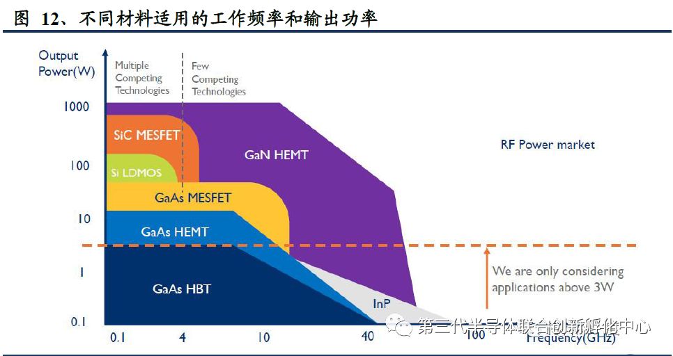
Gallium Nitride (GaN): theoretically has significantly superior performance to GaAs, making it GaAs devices’ biggest potential competitor. GaN has a bandgap of 3.4eV, which is significantly higher than the first-generation semiconductor Si and the second-generation semiconductor GaAs. The critical breakdown voltage is also higher than that of other semiconductor materials, while GaN also has higher saturation electron velocity, can operate at higher frequency bands, adapt to higher operating temperatures, and theoretically outperforms GaAs, making GaN an important competitor to GaAs devices.
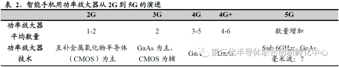
Silicon (Si): the first-generation semiconductor material, as RF devices gradually evolve towards high frequency and high power, its application is increasingly limited due to performance constraints. On one hand, Si has lower saturation electron velocity and electron mobility, with relatively poor high-frequency characteristics; on the other hand, high-frequency losses are higher when using Si as a substrate. Additionally, the relatively low breakdown voltage is the biggest drawback of Si materials, making it difficult to adapt to the design of high-power RF devices. From the evolution of smartphone power amplifiers, Si-based CMOS dominated in the 2G era, but by the 3G era, the market share of CMOS began to decline. With the application scenarios of RF devices further evolving towards high frequency and high power, the market share of Si-based CMOS in the smartphone power amplifier market is expected to decline further due to its performance limitations.
Silicon Carbide (SiC): a third-generation semiconductor material, currently the substrate has been developed well, but it is difficult to continuously excite solely with silicon carbide. Currently, it seems challenging to apply it in RF devices. It has good application prospects in replacing Si’s IGBT in high-speed rail and electric vehicles.
Indium Phosphide (InP): belongs to the second generation of semiconductor materials along with GaAs, with similar basic performance. However, due to its fragile substrate and difficulty in processing, it is challenging to produce RF devices and replace GaAs. Its main applications remain in fiber optic communication and laser detectors.
Silicon Germanium (SiGe): due to its narrow bandgap, cannot be applied in high-frequency fields, and is mainly used in small-scale cordless phones and Bluetooth.
2.2.2 From the Perspective of Technological Maturity, GaN Substrates Have a Long Way to Go to Replace GaAs
The GaN industry is still in its infancy, with high difficulty in substrate production and slow technological progress. Currently, the technologies for fabricating GaN substrates include Hydride Vapor Phase Epitaxy (HVPE), Ammonothermal Method, Sodium Flux Method, and High-Pressure Growth Method.
-
HVPE method involves epitaxially growing GaN on substrates such as sapphire or GaAs, and subsequently separating the original substrate from the epitaxial layer and performing polishing and other processing to obtain GaN substrates. However, due to the heteroepitaxial growth process, lattice mismatch and thermal mismatch can easily occur between the GaN epitaxial film and the original substrate, leading to high residual stress, cracking, warping, and other issues in the epitaxial film, affecting yield.
-
The ammonothermal method faces challenges in controlling crystal growth conditions in actual production, and wafer size is also limited.
-
Both the sodium flux method and high-pressure growth method have stringent requirements for equipment and processes, and significant breakthroughs in single crystal size are also difficult to achieve.
High costs limit the commercialization of GaN substrates. Due to the high difficulty of production processes, low yield, and slow technological research and development progress, the cost of GaN substrates remains high. In 2005, the cost of a 2-inch substrate was $20,000, and after 15 years of development, the substrate price is still at the level of $3,000, while the cost of a 4-inch GaAs substrate is only 100-200 yuan at low-end prices, and a 2-inch GaAs substrate costs only a few dozen yuan. The cost issue greatly restricts the commercialization of GaN as a substrate.
At least for now, Sub-6GHz mobile RF devices are still the main battlefield for GaAs. However, as it develops into the higher frequency millimeter-wave stage in the medium to long term, GaAs, due to its lower thermal conductivity and poorer heat dissipation, will likely struggle to meet the power requirements of RF devices above 28GHz, and will probably need to use materials with GaN as the working layer. Whether GaN, suitable for higher frequency applications, can smoothly take over remains to be seen, pending breakthroughs in technology and cost.
2.3 Where Does GaN Stand as a Dual Titan?
In the short term, although GaN as a substrate material finds it difficult to achieve rapid technological and cost breakthroughs for commercialization, as an epitaxial material, GaN can already be epitaxially grown on substrates such as silicon carbide, silicon, sapphire, and diamond.
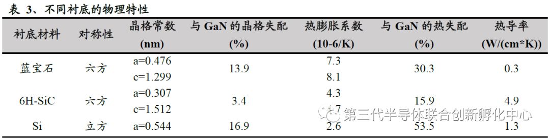
① SiC substrate: The advantage of SiC as a substrate material is that the lattice mismatch and thermal mismatch rates between SiC and GaN are smaller compared to Si substrates and sapphire substrates, while SiC has high thermal conductivity, making it suitable for growing high-quality GaN epitaxial layers to meet high-power applications. However, SiC substrates face issues such as high prices, poor mechanical processing performance, and high defect density. Currently, producing high-quality, large-size SiC single crystals remains challenging.
② Si substrate: Si substrates have large diameters and are easy to process, offering absolute advantages in price, allowing larger wafers to be processed while ensuring low costs. However, the lattice mismatch and thermal mismatch rates between Si and GaN are larger, making it challenging to grow high-quality GaN, generally only suitable for small power devices.
③ Sapphire (Al2O3) substrate: Sapphire has a wide bandgap, good chemical stability, and thermal stability, allowing for growth at high temperatures. Additionally, the production technology for sapphire substrates is relatively mature and comparatively inexpensive, providing certain cost advantages. However, the lattice mismatch and thermal mismatch rates between sapphire and GaN are relatively large, leading to poor conductivity and thermal conductivity, which significantly affects high-current performance in large power devices. Currently, sapphire as a substrate material for RF devices has been eliminated.
④ Diamond substrate: Diamond has a thermal conductivity over four times that of SiC, along with higher critical breakdown voltage, larger bandgap, and higher electron mobility. GaN RF devices with diamond substrates are expected to achieve superior performance. However, due to the significant lattice mismatch and thermal mismatch rates with GaN, the heteroepitaxial growth of GaN remains challenging.
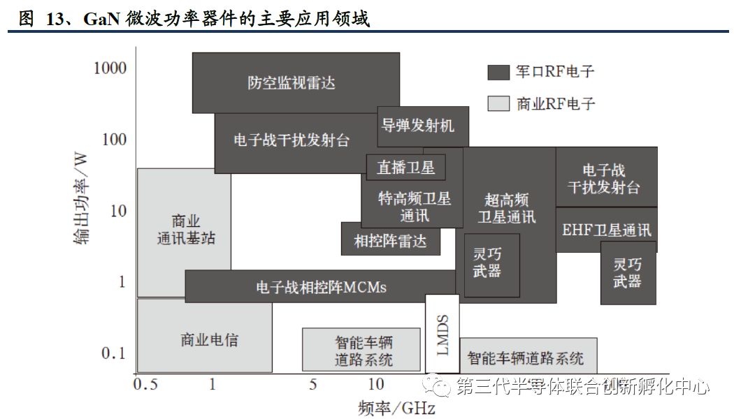
The application market for GaN microwave power devices includes defense, satellite communication, and wireless communication base stations. For the wireless communication base station market, we believe that with the arrival of the 5G era, GaAs is expected to remain the mainstream for indoor network system structures, but in the macro base station field, GaN will stand out due to its high power characteristics. From different processes, it is expected that GaN-on-SiC will become the mainstream semiconductor material for RF devices in macro base stations with high power requirements.
The prices of RF devices with GaN as the epitaxial layer have decreased, providing possibilities for large-scale applications in macro base stations. According to the “2018 Global Third-Generation Semiconductor Industry Development Review and Outlook” published by the Third-Generation Semiconductor Industry Technology Innovation Strategic Alliance in 2019, companies including Qorvo, Cree, NXP, and MACOM (where MACOM mainly produces GaN-on-Si RF devices, and Qorvo, Cree, and NXP mainly produce GaN-on-SiC RF devices) have sold 170 types of GaN HEMT RF devices, with product prices ranging from 90 to 9000 yuan each, averaging 23.78 yuan/W, which has fallen to within three times the average price of Si LDMOS (8.50 yuan/W). As the technological maturity of GaN-on-SiC production gradually improves, prices are expected to continue to decline, providing a foundation for large-scale applications in the RF field of macro base stations in the 5G era.
3. Estimating the Market Space for GaAs/GaN
(Considering only mobile phone and base station RF applications)
3.1 Mobile Phones: Upgrade Wave + Penetration Rate Increase + PA Quantity Increase, GaAs Demand Soars
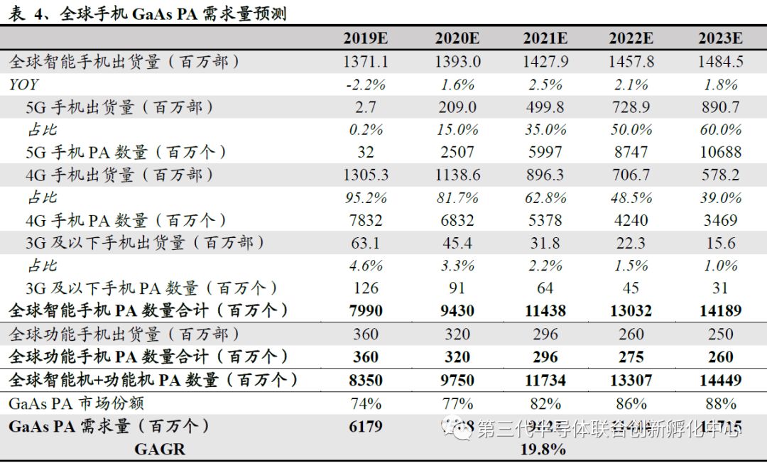
The 5G era stimulates upgrade demand, and the smartphone market is expected to return to a growth trajectory. Since 2015, the global smartphone market has entered a mature stage, becoming increasingly saturated, with declining innovation efforts, longer consumer upgrade cycles, and continuous declines in shipment volume. Globally, according to IDC data, in 2018, the global smartphone shipment volume was 1.395 billion units, down 4.8% year-on-year, but signs of market recovery began to emerge in the second half of this year, with a forecasted year-on-year decline narrowing to 0.4% in the second half, and the total annual shipment volume is expected to reach 1.3711 billion units, a year-on-year decline of 2.2%. Domestically, in 2018, the total domestic smartphone shipment volume was 414 million units, down 15.6% year-on-year, and the shipment volume in the first three quarters of 2019 was 287 million units, down 5.7% year-on-year, with the decline having narrowed. We believe that with the advancement of 5G, the demand for consumer upgrade will be stimulated, and the decline in smartphone shipment volume is expected to be reversed. According to IDC forecasts, global smartphone shipments are expected to stop declining and grow by 1.6% year-on-year in 2020, reaching 1.4845 billion units by 2023, with a GAGR of 1.1% from 2018 to 2023.

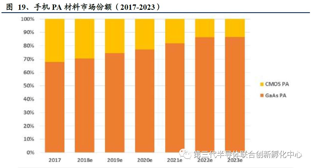
GaAs is expected to continue to increase its market share in mobile phone PAs. Si-based CMOS has significant performance limitations due to its smaller bandgap, weaker breakdown electric field, and lower electron mobility and saturation electron velocity, making it increasingly difficult to adapt to the evolving application scenarios of RF devices towards high frequency and high power. Meanwhile, GaN-based RF devices with better performance are still facing challenges for commercialization due to technological and cost issues. The Sub-6GHz stage of the 5G era will still be the main battlefield for GaAs materials, with GaAs PAs expected to continue capturing market share from Si-based CMOS, further increasing penetration rates.
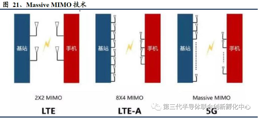
The number of PAs per device is expected to increase significantly. Generally, 3G and earlier mobile phones are equipped with 1-2 PAs, while 4G phones have an average of 3-6 PAs. By the time of the 5G era, due to the increase in new frequency bands and the application of Massive MIMO (large-scale multiple input multiple output) technology, the number of antennas on mobile devices is expected to increase significantly, leading to a corresponding increase in the number of PAs per mobile phone, expected to reach more than 10.
Upgrade Wave + Penetration Rate Increase + PA Quantity Increase, GaAs Demand Soars. We predict that from 2019 to 2023, the demand for GaAs PAs for global smartphones and feature phones will increase from 6.18 billion units to 12.7 billion units, with a GAGR of 19.8%. Even considering the trend toward miniaturization, the demand for GaAs PAs is still expected to grow significantly in the coming years.
3.2 Base Stations: Rapid Growth in Numbers, GaAs and GaN Each Take the Lead
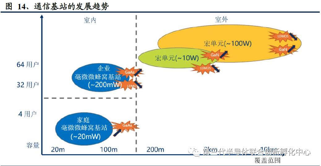
In the 5G era, network coverage will be achieved mainly through “macro base stations as the mainstay and micro base stations as support,” with GaAs and GaN RF devices each taking the lead. Due to the higher frequency bands of 5G solutions compared to the currently mainstream 4G bands, the corresponding wavelengths are significantly reduced, leading to poorer diffraction capabilities and greater path loss, meaning that the transmission distance of 5G is shorter and coverage capability is significantly weakened compared to 4G. Solving this issue will require the construction of more base stations. At the same time, considering cost factors, “macro base stations + micro base stations” will be the ideal solution. In terms of RF material selection, micro base stations are smaller and have relatively lower power consumption requirements, so GaAs will become the mainstream, while macro base stations will primarily use GaN-based materials.
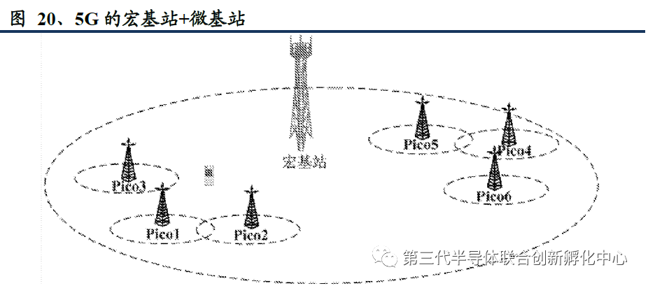
The application of Massive MIMO technology requires a significant increase in the number of PAs per base station. Massive MIMO is a very important technology in the 5G era, which increases the spectral efficiency, coverage capability, and network capacity of communication systems by using a large array of antennas at the base station. This requires corresponding RF transceiver unit arrays to match, resulting in a significant increase in the number of PAs per base station. If 4G era antenna arrays are mainly 4T4R and 8T8R, assuming that 5G base stations commonly adopt 64T64R antenna arrays, then with the evolution from 4G to 5G, the number of PAs per base station is expected to increase by 8-16 times, which will undoubtedly bring huge demand increases for GaAs and GaN materials.
The increase in the number of base stations + the multiplication of the number of PAs per base station will lead to a significant increase in the demand for GaAs and GaN. In addition, in the application of macro base stations, GaN holds a significant advantage in high-frequency and high-power performance, and is expected to continue capturing market share from LDMOS, further increasing demand.
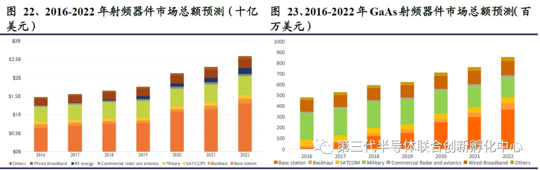
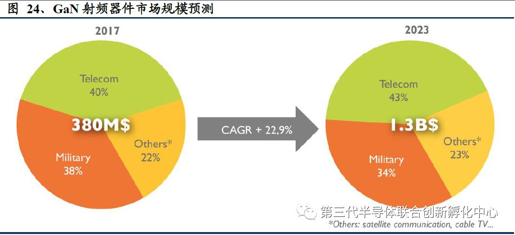
According to Yole’s predictions, the total market size for GaAs RF devices is expected to grow from $481.6 million in 2016 to $857.6 million in 2022, with a GAGR of 10.1%. Among them, the market size for base station applications will grow from $15.3 million in 2016 to $37.07 million in 2022, with a GAGR exceeding 70%. Yole also predicts that the market size for GaN RF devices will grow from $380 million in 2017 to $1.3 billion in 2023, with a GAGR exceeding 20%, with the primary growth coming from base station applications.
4. Applications of GaAs in the Optoelectronic Field
4.1 LEDs: Large Volume, Expected to Continue Steady Growth
LEDs are currently the second-largest application market for GaAs substrates, next to RF applications, and are expected to continue steady growth in the coming years.
-
Depending on the application wavelength, they can be divided into red, orange, yellow LEDs and infrared LEDs. Red, orange, and yellow LEDs are mainly used in lighting and display applications, where GaAs maintains a solid low position with little threat from other technologies. Infrared LEDs correspond to medical, remote control, optical communication, and other applications, with a market that is significantly smaller than red, orange, and yellow LEDs.
-
Based on different technical specifications (defect density, carrier concentration, etc.), they can be divided into low-end LEDs and high-end LEDs. Low-end LED substrates are typically used for certain displays, signal lights, and decorative lighting, while high-end LED substrates are used in high-brightness and high-precision applications.
-
GaAs LED devices are currently only used as switches in mobile phones, but the application of GaAs in infrared LEDs for smartphones is expected to see noticeable growth. According to Yole, from 2017 to 2023, the shipment volume of GaAs substrates for infrared LEDs in smartphones is expected to increase from 28,600 units to 49,200 units, with a GAGR of 9%, and the market total is expected to rise from $2.22 million to $3.4 million, with a GAGR of 7%.
-
In addition to traditional LEDs, micro-LEDs and mini-LEDs are also continuously developing, with micro-LEDs primarily used in smartphone backlighting.
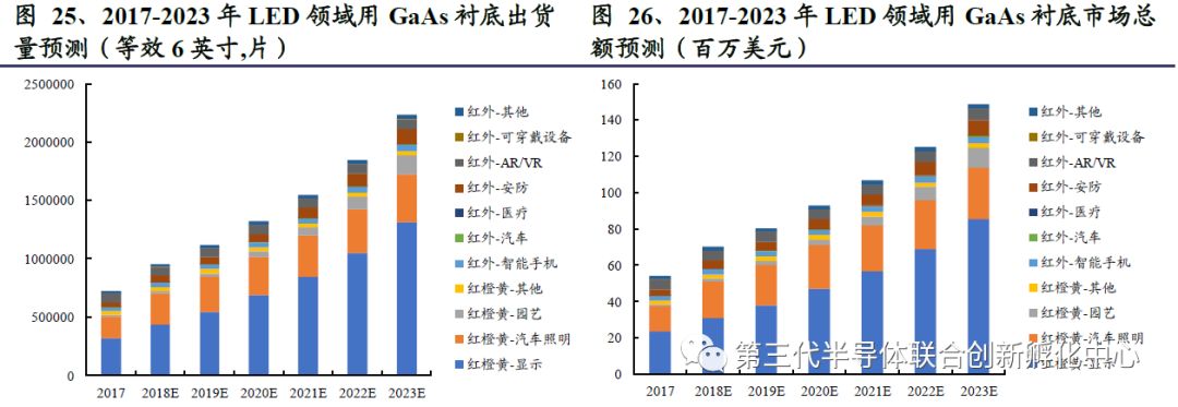
According to Yole, traditional displays, automotive lighting, and other fields using GaAs substrates are large in volume and are expected to continue steady growth. The application of GaAs-based red, orange, and yellow LEDs in horticultural lighting (for plant growth) is growing rapidly. Additionally, infrared applications in security and smartphones are also expected to see good growth. By 2023, the shipment volume of GaAs substrates in the LED field is expected to rise from 725,000 units in 2017 to 2,238,000 units, with the market total expected to increase from $54 million to $149 million from 2017 to 2023.
4.2 Lasers: From Non-Existence to High Growth Expected for VCSEL
GaAs applications in the laser field can be divided into VCSEL and non-VCSEL, with the current focus on VCSEL applications. VCSEL (Vertical-Cavity Surface-Emitting Laser), based on GaAs material, is primarily used for facial recognition, representing a process from non-existence to existence, and is expected to see high growth in the future. EEL (Edge-Emitting Laser) belongs to non-VCSEL devices and is mainly applied in automotive laser radar, with demand expected to increase with the expansion of the autonomous vehicle market.
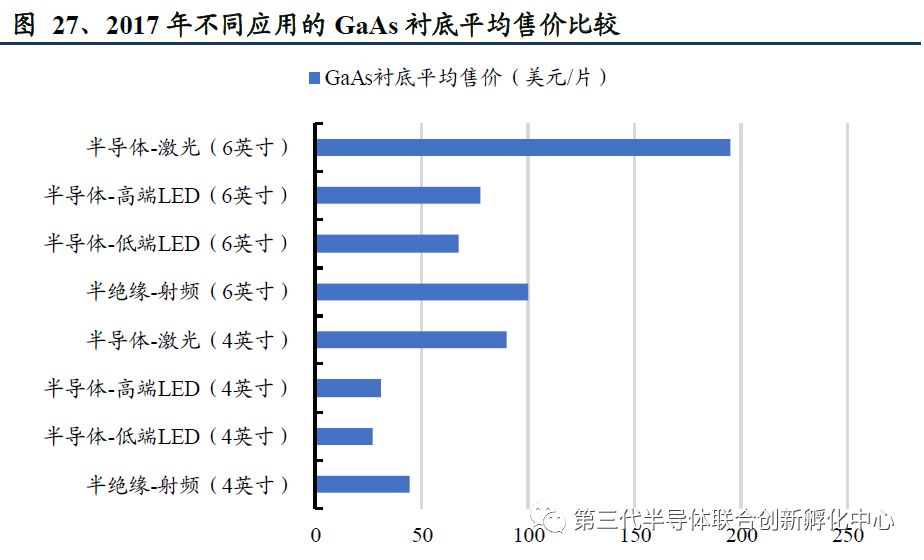
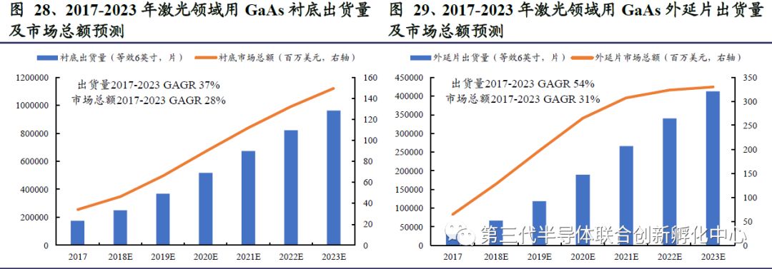
The technical specifications required for GaAs substrates in the laser field are high, with prices significantly higher than in other fields, indicating promising market space in the future. Laser applications are most sensitive to dislocation density and have the highest requirements for GaAs substrate materials, leading to significantly higher prices for GaAs substrates of the same size used for lasers compared to other fields. According to Yole, the shipment volume of GaAs substrates in the laser field is expected to rise from 175,000 units in 2017 to 964,000 units by 2023, with a GAGR of 37%, and the market total expected to increase from $34 million in 2017 to $150 million by 2023, with a GAGR of 28%.
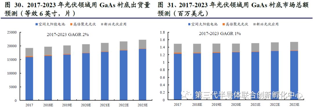
4.3 Photovoltaics: Niche Market, Expected Low Growth Rate
GaAs applications in space photovoltaic power generation are facing competition from Ge substrates, and are expected to see low growth rates in the future.
5. An Oligopoly Market Dominated by Overseas Players,
Domestic Production Begins to Replace Imports
5.1 Global Competitive Landscape: An Oligopoly Market Dominated by Overseas Players
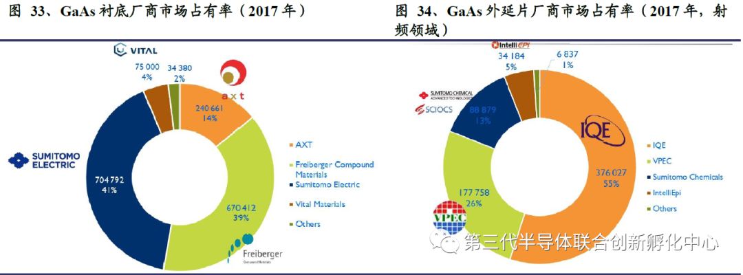
GaAs: Due to the high technical barriers in the RF field for GaAs, the PA market is characterized by very high concentration, with materials and designs being dominated by overseas companies. From the global GaAs industrial chain perspective, both the substrate and epitaxial wafer markets are monopolized by a few overseas companies. In 2017, the market shares of the three companies, Ferrotec, Sumitomo Electric, and AXT, in the GaAs substrate market reached 94%. In the RF market for GaAs epitaxial wafers, the outsourcing ratio for 6-inch epitaxial wafers is about 90%, with the two giants in the outsourcing field being IQE and Qorvo, holding market shares of 55% and 26%, respectively. Currently, Chinese GaAs substrate manufacturers mainly occupy the low-end LED market (decorative infrared LEDs, signals, etc.), with only a few GaAs substrate manufacturers able to supply substrates for high-end LED markets (infrared LEDs for automotive and horticultural lighting).
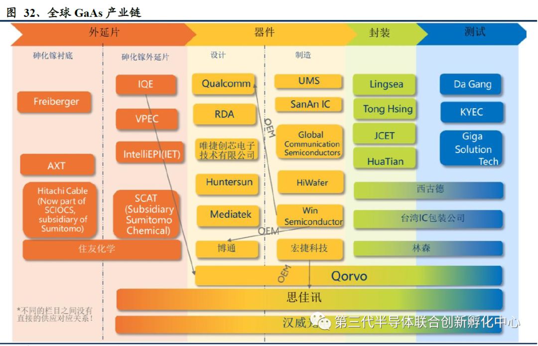
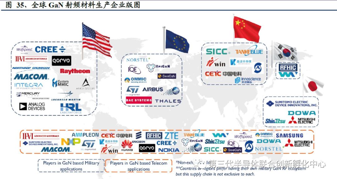
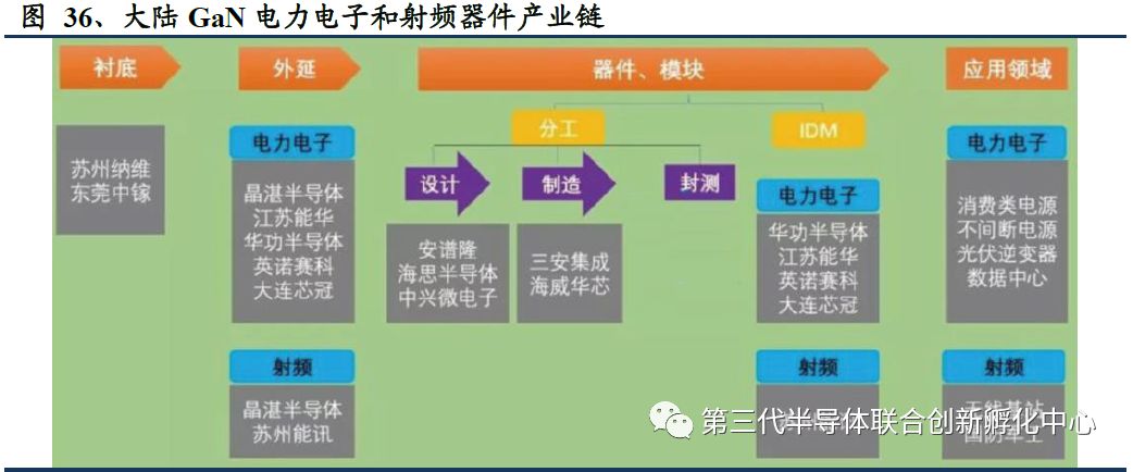
GaN: Compared to GaAs, it is an emerging market where R&D and production are still led by foreign manufacturers. Overseas companies such as Cree, Qorvo, MACOM, and MMIC are leading in technological development and product innovation. Mainland China now has a complete industrial chain layout covering GaN material substrates, epitaxy, process processing, circuit design, packaging, testing, modules, and reliability testing, with frequency bands covering 3mm and below, and some products reaching internationally leading levels. The main GaN substrate production companies for RF applications include Suzhou Navi and Dongguan Zhonggan, while the main epitaxy companies include Jingzhan Semiconductor and Suzhou Nengxun.
5.2 The Clear Trend of Self-Control, Starting the Domestic Replacement Process
The trend of self-control is clear, starting the domestic replacement of semiconductor materials. Whether in RF chips, lasers, or LED devices, the material manufacturing segment is the core value of the industrial chain, which is currently highly monopolized by overseas companies. Under the influence of the China-US trade conflict and the “Huawei incident,” the awareness of domestic production and independent brand building is continuously rising. With the clear trend of self-control, the GaAs and GaN semiconductor material industries are expected to receive policy support and resonate with industrial upgrades.
6. Related Listed Companies for GaAs/GaN Materials
6.1 Youyan New Materials: Positioning in the High-End LED Market
Youyan New Materials mainly engages in the R&D and production of rare earth materials, thin film materials for optoelectronics, biomedical materials, rare metals and precious metals, infrared optical and optoelectronic materials, optical fiber materials, and other new materials. Its important subsidiary, Youyan Optoelectronic New Materials Co., Ltd., mainly engages in the R&D and production of infrared optical and optoelectronic materials, serving as an important R&D center and production base for advanced semiconductor materials and infrared optical materials in China, with a globally leading infrared germanium single crystal production line, making it a major supplier of infrared optical germanium wafers and infrared LED substrate wafers.
Currently, Youyan Optoelectronic has an annual production capacity of 600,000 GaAs substrates, using horizontal GaAs single crystal production lines with excellent product uniformity, positioning in high-end LED applications with high added value, and is one of the main suppliers of GaAs-based substrates for infrared LEDs globally.
6.2 Yunnan Germanium Industry: Layout of GaAs and InP Materials
Yunnan Germanium Industry currently mainly produces zone-melted germanium ingots and germanium dioxide as its leading products; in deep processing, the photovoltaic-grade germanium products are mainly solar germanium substrate wafers, while the infrared germanium series products include infrared-grade germanium (optical components), germanium lenses, and infrared thermal imaging devices. The optical fiber-grade germanium products are germanium tetrachloride for fiber optics, while the non-germanium semiconductor materials mainly include GaAs single crystal wafers. The company’s GaAs single crystal production capacity is 800,000 wafers/year (equivalent to 4 inches), and in the first half of 2019, it produced 41,700 GaAs single crystal wafers (equivalent to 4 inches). Currently, the company is still mainly producing 4-inch wafers, and 6-inch GaAs has not yet been produced in bulk, with products mainly sold to South Korea, Fujian, Taiwan, and other regions. In the first half of 2019, the company’s non-germanium semiconductor material products (GaAs, InP) achieved operating revenue of 5.4178 million yuan, accounting for a small proportion of the total revenue, only 2.36%.