Unisoc Tongchuang PCIE Tutorial

Recently, Xiaoyanjing Technology launched a free trial activity based on the Unisoc Tongchuang Logos series PGL50H Pangu 50K development board. In the near future, I will successively present a series of experience reports. This issue shares insights from an FPGA engineer engaged in microelectronic chip design: Death God Durant. This issue presents: Experience with Unisoc Tongchuang PCIE DMA Read/Write and PIO Memory Read/Write TLP Analysis.

Unisoc Tongchuang PCIE Tutorial

1: PIO Memory Read/Write Operation TLP Analysis

Unisoc Tongchuang PCIE Tutorial
PCIE has three spaces – memory space, IO space, and configuration space, among which memory space is the commonly used space for PCIE devices, IO space is for compatibility with previous PCI devices (PCIE devices rarely use IO space now), and configuration space is the information space of PCIE devices (ID, BAR, etc. are written inside, and the host kernel program initializes by reading the configuration space information of PCIE, thus allocating PCI bus domain space to the Endpoint and other operations).
PIO does not mean reading and writing IO space; the principle is still reading and writing memory space. PIO read/write is similar to reading and writing registers, where data (generally 32bit) is written to a specific memory address each time. The operations of reading and writing PIO using official driver instructions are essentially the same as using WinDriver to operate Read/Write Memory, but the official driver limits the data length for each operation to 1DW (32bit), and data larger than 1DW will be sent multiple times.

Unisoc Tongchuang PCIE Tutorial

Write 1DW data.

Unisoc Tongchuang PCIE Tutorial

Write 2DW data.

Unisoc Tongchuang PCIE Tutorial

Write 3DW data.

Unisoc Tongchuang PCIE Tutorial

Read 1DW data.
Unisoc Tongchuang PCIE Tutorial
Read 2DW data.

Unisoc Tongchuang PCIE Tutorial

Read 3DW data.

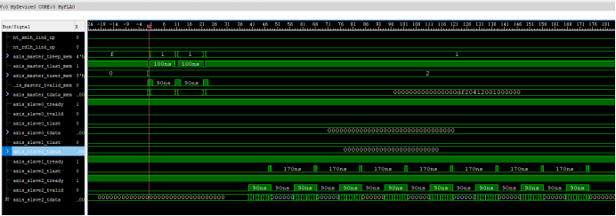
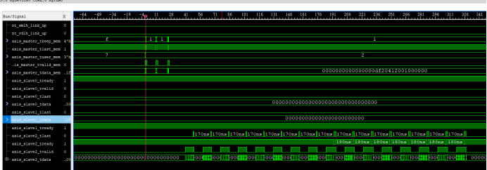
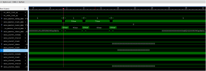
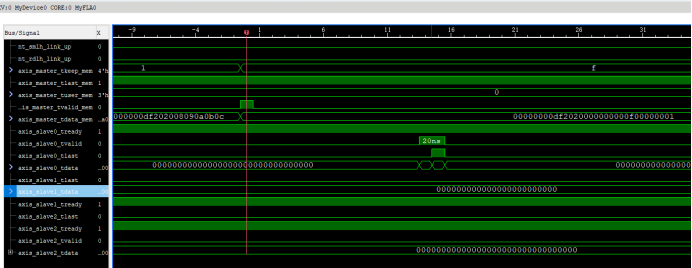
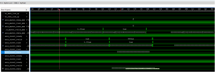
Note that according to the PCIE protocol’s Mwr, the maximum data size for a single Mwr/Mrd can be 4096Bytes. The above data larger than 4Bytes is sent in multiple Mwr operations, which is the driver’s approach. The timing diagram shows that the signals meet the requirements, but what about the actual data of the signals? Now let’s analyze these data by taking reading and writing 12Bytes of Memory as an example.

Write/Read Memory uses three types of messages – Mwr/Mrd/CplD. When using the PCIE IP, the underlying details can be overlooked, but parsing the received TLP and sending compliant TLP is the focus.

For Mwr/CplD, the data they carry is the data itself, and there is nothing to analyze; the focus is on the Header in the TLP. The Mrd message only has a Header, so analyzing the Header is the key.

Note that Mwr/Mrd is address routing, while CplD is ID (Bus/Device/Function) routing. This is stipulated by the protocol. The so-called routing can be simply understood as the RC being able to send the data to the target device based on the address/ID among numerous PCIE transmission paths because the kernel program initializes and allocates PCIE bus domain space for each BAR, and each BAR space address is independently mapped, while the ID uniquely determines based on (Bus/Device/Function).

The Header format for Mwr/Mrd is as follows:

Unisoc Tongchuang PCIE Tutorial

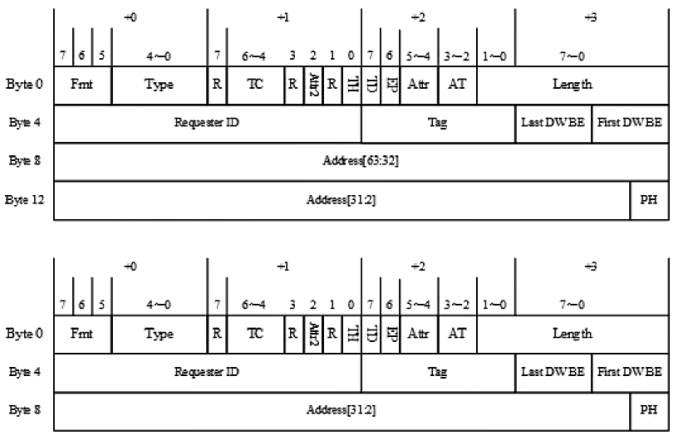
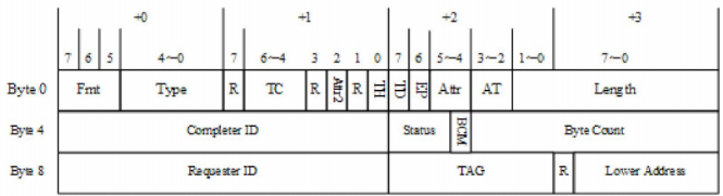
The Header format for CplD is as follows:

Unisoc Tongchuang PCIE Tutorial

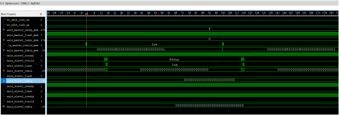
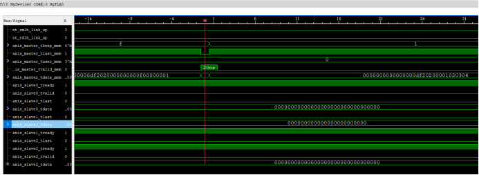
Mwr:Header:0x0000_0000_df20_2000_0000_000f_4000_0001Data: 0x0000_0000_0000_0000_0000_0000_0102_0304Header:0x0000_0000_df20_2004_0000_000f_4000_0001Data:0x0000_0000_000_0000_0000_0000_0506_0708Header:0x0000_0000_df20_2008_0000_000f_4000_0001Data:0x0000_0000_0000_0000_0000_0000_090a_0b0c
For the Mwr Header, analyzing against the protocol format makes it easy to know that the first Header address (32bit) is df20_2000, the data length Length (in DW) is 1, and the message type [Fmt,Type]=0x40 (indicating a 3DW Mwr), byte enable [last DW BE,first DW BE]=0x0f. Other information can be filled in as needed, and it is particularly important to note that TLP is in big-endian format, [Fmt,Type]=axis_master_tdata[31:24], which actually represents the position of 0Byte, and other DW data is similar.
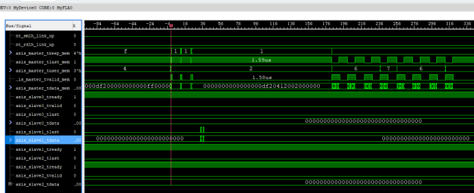
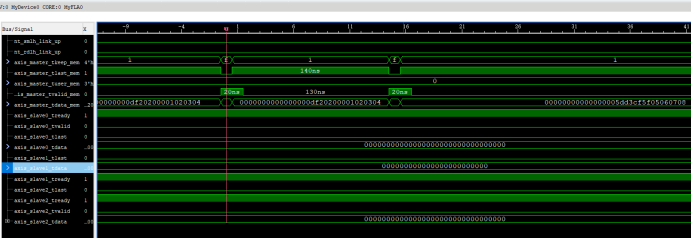
Mrd:Header:0x0000_0000_df20_2000_0000_000f_0000_0001Header:0x0000_0000_df20_2004_0000_000f_0000_0001Header:0x0000_0000_df20_2008_0000_000f_0000_0001
For the Mrd Header, analyzing against the protocol format makes it easy to know that the address (32bit) is df20_2000, the requested data length Length (in DW) is 1, and the message type [Fmt,Type]=0x00 (indicating a 3DW Mrd), byte enable [last DW BE,first DW BE]=0x0f. Other information can be filled in as needed, and for further understanding, refer to the PCIE protocol specification.
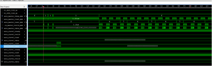
CplD:Header:0x0000_0000_0000_0000_0100_0004_4a00_0001Data:0x0000_0000_0000_0000_0000_0000_0102_0304Header:0x0000_0000_0000_0010_0100_0004_4a00_0001Data:0x0000_0000_0000_0000_0000_0000_0506_0708Header:0x0000_0000_0000_0020_0100_0004_4a00_0001Data:0x0000_0000_0000_0000_0000_0000_090a_0b0c
For the CplD Header, it uses ID routing, making it easy to know that the Requester ID is 0x0000, the Completer ID is 0x0100, the reply data length Length (in DW) is 1, and the message type [Fmt,Type]=0x4a (indicating CplD). The Byte Count is 0x004, TAG is 0x00, and other information can be filled in as needed. The specific meanings can be found in the PCIE protocol specification.
Unisoc Tongchuang PCIE Tutorial
2: DMA Read/Write Operation TLP Analysis
Unisoc Tongchuang PCIE Tutorial
DMA (Direct Memory Access) is initiated by the FPGA, so the host must send data to the FPGA. First, it sends a DMA read command and the starting address of the data in the host memory to the FPGA. The FPGA initiates an Mrd based on the memory starting address and data length, and the host replies with a CplD, thus transferring the data to the FPGA, known as DMA read operation. Conversely, the host sends a DMA write command and the data to be placed at the host memory starting address to the FPGA. The FPGA initiates a data-carrying Mwr based on the memory starting address and data length, thus transferring the data to the host, known as DMA write operation.

Unisoc Tongchuang PCIE Tutorial

1024Byte DMA read, from host to FPGA.
Unisoc Tongchuang PCIE Tutorial
1024Byte DMA write, from FPGA to host.

Unisoc Tongchuang PCIE Tutorial

2048Byte DMA read, from host to FPGA.

Unisoc Tongchuang PCIE Tutorial

2048Byte DMA read, from FPGA to host.

From the above DMA read/write timing diagrams, it is not difficult to see that to achieve DMA read, the host will first send 3 Mwr TLPs to the FPGA. After parsing the Mwr TLP, the FPGA will initiate an Mrd TLP, and the host will then reply with a CplD TLP, thus transferring the data to the FPGA; to achieve DMA write, the host will first send 3 Mwr TLPs to the FPGA. After parsing the Mwr TLP, the FPGA will directly send a data-carrying Mwr TLP, thus transferring the data to the host.
What are the 3 Mwr TLPs from the host? By interpreting the DMA module under the dma_controller module of the example routine, it is not difficult to find that the data at BAR1+0x100 offset indicates whether the FPGA initiates a data-carrying Mwr or a non-data-carrying Mrd (including data length, etc.), the data at BAR1+0x100 offset is the low 32 bits of the physical memory starting address of the host carrying the data, and the data at BAR1+0x100 offset is the high 32 bits of the physical memory starting address of the host carrying the data.
DMA is direct memory access, which requires direct data transfer/write from the host memory. First, the host memory starting address must be known. Is it always 3 Mwr TLP communications handshake? Definitely not; this is the method of generating the IP routine. If you design your own DMA controller, you can use a more complex/more efficient handshake mechanism to trigger DMA operations.
The timing diagram Header:
DMA – Host’s Mwr (Taking 1024Byte as an example)
First: Header:0x0000_0000_df20_4100_0000_000f_4000_0001Data:0x0000_0000_0000_0000_0000_0000_ff00_0100
Second: Header:0x0000_0000_df20_4110_0000_000f_4000_0001Data:0x0000_0000_0000_0000_0000_0000_00a0_2647
Third: Header:0x0000_0000_df20_4120_0000_000f_4000_0001Data:0x0000_0000_0000_0000_0000_0000_0100_0000
This Mwr is 32bit Address access, and memory access is routed through addresses. The significance of the Header is consistent with the analysis of the above Mwr.
DMA – Host’s CplD (Taking 1024Byte as an example)
1st Header:0x0000_0000_0100_0000_0000_0200_4a00_0020
2nd Header:0x0000_0000_0100_0000_0000_0180_4a00_0020
3rd Header:0x0000_0000_0100_0000_0000_0100_4a00_0020
4th Header:0x0000_0000_0100_0000_0000_0080_4a00_0020
5th Header:0x0000_0000_0100_0100_0000_0200_4a00_0020
6th Header:0x0000_0000_0100_0100_0000_0180_4a00_0020
7th Header:0x0000_0000_0100_0100_0000_0100_4a00_0020
8th Header:0x0000_0000_0100_0100_0000_0080_4a00_0020
The completion message uses ID routing (as stipulated by the protocol, simply put, each BAR has its own ID (Bus/Device/Function), and through this unique ID, the recipient can be found).
The CplD Header can only consist of 3DW, which is consistent with the above CplD analysis. It should be noted that the protocol stipulates that the maximum data length of CplD is 1024DW (4096 Bytes), but the Max Payload Size set by our IP configuration page is actually 128 Bytes, so data larger than 128 Bytes needs to be sent in multiple segments. It should be noted that the TAG of the first 4 Headers is 0x00, and the TAG of the last 4 Headers is 0x01. Why is this? Because the FPGA sent two Mrd requests, and the TAG records that the Mrd was sent, and the TAG in the received completion message is consistent with the Mrd, indicating that the current Mrd has been completed.
It can be seen that the TAG is 8 bits. Once the TAG of the Mrd is 0xff, but the CplD with TAG=0x00 has not yet replied, the Mrd cannot be sent again (for the same BAR’s Mrd).
It can be seen that the Byte Count changes, which is easy to understand, indicating how much of the requested data from the Mrd is still left to be transferred (here it is not our final 1024 Bytes, but the Byte count of one Mrd). The first Header is 0x200, indicating that there are still 512 Bytes left to transfer from the Mrd request, the second Header is 0x180, indicating that there are still 384 Bytes left to transfer from the Mrd request, and so on. The fifth Header returns to 512 Bytes because the fifth Header CplD is a new Mrd request, also requesting a length of 512 Bytes.
DMA – FPGA’s Mrd (Taking 1024Bytes as an example)
Header:0x20d5_0400_0000_0000_0000_0001_0100_1c80Header:0x20d5_0480_0000_0000_0000_0001_0100_3c80
This Mrd is 64bit Address access, and memory access is routed through addresses. The significance of the Header is consistent with the analysis above. This 64bit address is the address at which the FPGA wants to read the host’s memory, with the low 32 bits in the 4th DW and the high 32 bits in the 3rd DW. This address is certainly not fixed; even on the same computer, the location where the host allocates memory space for data varies each time.
Why does the Mrd need to be sent in two parts? Because the Max_rd_req_size set by the PCIE IP is 512 Bytes, so data larger than 512 Bytes requires multiple Mrd requests. For example, to request 2048 Bytes of data from the host memory, 4 Mrd requests are needed, each recording a Tag, corresponding to the Tag of the CplD.
DMA – FPGA’s Mwr (Taking 1024Bytes as an example)
The Mwr has already been elaborated multiple times, so I will not repeat it.
Unisoc Tongchuang PCIE Tutorial

Unisoc Tongchuang PCIE Tutorial

Unisoc Tongchuang PCIE Tutorial
Pangu 50K Development Board | Unisoc Tongchuang PGL50H Development Platform
Unisoc Tongchuang PCIE Tutorial
For related supporting routine materials, please contact WeChat customer service: 17665247134
Welcome to join the FPGA Developer Technical Community!
FPGA Developer Technical Community link: https://bbs.elecfans.com/xfpga

END

Leave a Comment