Authors: J. Brunning and R. Rayit, SARAS Technology, Leeds, U.K.
The design method for broadband, linear, and efficient output-backoff mode RF power amplifiers (RFPA) emphasizes the importance of minimizing design uncertainty. Using this approach, excellent consistency between modeling and measurement performance can be achieved on the first design.
The demand for linear RFPAs covering the frequency range of 1.5 to 2.8 GHz is driving new design approaches for broadband, linear, and efficient RFPAs operating in output-backoff mode. For a long time, improving the efficiency of power amplifiers has been a challenge for designers, partly due to poor harmonic load impedance control. The difficulty of measuring waveforms at microwave frequencies makes it hard to determine whether optimal waveform shaping has been achieved. When harmonics at lower operating frequencies fall within the operating band, broadband designs increase the challenge. Inaccurate design techniques exacerbate these inherent difficulties, leading to time-consuming and costly iterations.
This article describes the design process using the NI AWR Design Environment platform (specifically, the Microwave Office circuit design software), along with measurement techniques used to determine the input and output impedance of the matching network before the RFPA is powered on. Several methods are proposed to address the inherent issues in PA design, with the aim of minimizing uncertainty and achieving first-time success.
The effectiveness of this approach is demonstrated using a commercial discrete 10 W GaN on SiC packaged high electron mobility transistor fabricated with a 0.25 µm process (Qorvo’s T2G6000528) and a 20 mil RO4350B printed circuit board. The manufactured RFPA achieves greater than 40 dBm peak power and greater than 54% peak drain efficiency across its operating bandwidth. In output-backoff mode, when driven by a 2.5 MHz, 9.5 dB peak-to-average power ratio (PAPR) COFDM signal in the 2.0 to 2.5 GHz frequency range, the RFPA achieves 30 dBc of uncorrected linearity and 34% or higher drain efficiency.
RFPA Design Process
Device Selection
The first step begins with a thorough device/technology selection process to identify the best candidate devices to meet a specific set of criteria before engaging in time-consuming load and source pulling and network synthesis tasks. Several candidates are acceptable based on the claimed frequency and power. In addition to more common characteristics such as V ds, gain, operating frequency, and rated power, other parameters like C ds, C gs, and transformation ratios are also considered.
Optimal Load Impedance Extraction
Once the device is selected and a nonlinear model is obtained, the optimal source and load impedances can be determined. The load impedance required to achieve maximum power, efficiency, and gain (or acceptable trade-offs between these performance metrics) depends on frequency and varies significantly within the operating bandwidth of the broadband design.
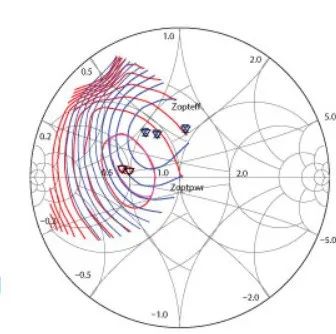
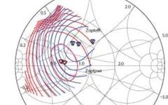
Figure 1 shows the power (red) and efficiency (blue) contour plots of the fundamental load pull analysis across the operating bandwidth.
To determine the correct load impedance, a combination of fundamental and harmonic frequency load pull mapping and waveform engineering (based on circuit design techniques shaping the voltage and current waveforms of the transistor) was performed in Microwave Office. The use of waveform engineering relies on accessing intrinsic device nodes through a current generator at the device plane rather than at the package reference plane. Assuming the nonlinear device model provides these nodes, the waveform engineering approach allows for visual observation of voltage and current swing, clipping, and amplifier operation categories.
For this example, load pull simulations were run at V ds = +28 V and I dq = 90 mA across the entire operating bandwidth, extracting the impedance for optimal power and efficiency, with mid-band results shown in Figure 1. The target load area defined based on P max -1 dB and drain efficiency max (eff max ) -5% overlap indicates that a larger target area simplifies matching issues. In this case, P max occurs on a tightly arranged clockwise trajectory across the operating bandwidth, which is beneficial in the case of broadband amplifiers. Due to the broadband characteristics of the RFPA and the difficulty of achieving optimal harmonic termination without network transmission zeros, load pulling was performed at the fundamental frequency. Load pulling for the second harmonic was also performed, with the high-efficiency area identified as 1, which can be controlled in network synthesis.
Network Synthesis
The advantage of narrowband RFPAs is that the optimal load impedance changes little within its operating bandwidth, thus reducing the complexity of the network design task. This does not mean that low fractional bandwidth matching is always trivial. In fact, studying source and load impedances reveals that for extremely high performance, the network’s fundamental impedance typically must be precisely controlled to a single gamma point; if the network trajectory misses its target load impedance, significant suboptimal performance losses occur. The precise control of harmonic termination impedances for F and F -1 amplifier classes increases the complexity of the task beyond what is required for typical PA designs.
In the case of broadband amplifiers, especially those with high-performance specifications, the network must control its impedance variations over a larger fractional bandwidth. After defining the optimal impedance and target area, the load network is developed using Simplified Real Frequency Technique (SRFT) 3 to design an ideal lumped element network and convert it into a distributed stepped impedance format, 4 before performing electromagnetic (EM) simulations. In this case, the EM simulation results closely matched the model predictions; however, this may not be true for less conventional matching topologies. Typically, EM simulation is viewed as an important step in reducing uncertainty in the design process.
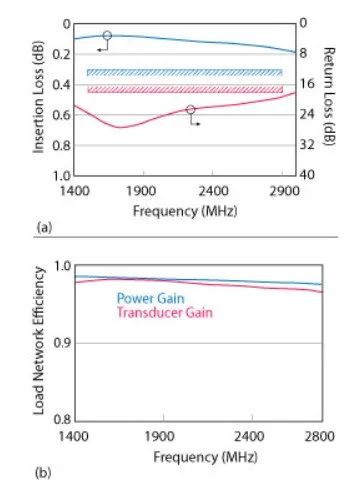
Figure 2 shows the relationship between distributed load network loss and matching (a) and the sensor and operating power gain versus frequency (b).
One design technique is to represent the optimal impedance as the conjugate of the generator at one port (Port 1), after which the matching network design can be viewed as a problem of minimizing the mismatch loss between that complex load and the 50 Ω termination on the amplifier’s operating bandwidth. However, this mismatch can be evaluated on the 50 Ω side of the network (Port 2), as shown in Figure 2a. As a passive network, the output matching circuit’s operating power gain is less than 1, determined solely by internal dissipative loss. The inevitably smaller transducer gain is the product of this efficiency and the losses caused by input reflection. These quantities are shown in Figure 2b as efficiency percentages. The efficiency of the load network is calculated to be 96.6% at 2800 MHz, close to the value calculated from the return loss at the same frequency. For comparison, the operating power gain considering only resistive losses in the network is calculated to have an efficiency of 97.7%. Although this does not directly include reflection losses, its value does depend on the terminal impedance, as they affect the distribution of current and voltage within the network, thus impacting copper and dielectric losses, respectively.
The transducer gain is evaluated against its impedance, which is the conjugate of the target load impedance seen by the device’s drain. Although output matching compresses power and efficiency rather than minimizing reflection at the drain, it was found that using conjugate matching closely aligns with the predicted compression power reduction due to imperfections in achieving the target load impedance. Thus, the plotted transducer gain is a good measure of the overall quality of output matching.
For several reasons, achieving optimal broadband matching with this transistor is relatively straightforward. First, the transformation ratio across the operating bandwidth is relatively low (about 2:1); second, the load impedance for optimal P max is closely arranged; and finally, the optimal impedance varies with increasing frequency along the clockwise rotating trajectory. The relatively low transformation ratio is a useful criterion for selecting this GaN device for broadband RFPA applications.
Figure 3 shows the DLL (a) and IV waveforms (b) at the internal device nodes with a 1500 MHz CW signal and 10 W output power.
Source Network
The source impedance variation across the operating bandwidth can be controlled using a band-pass filter network, which also has the advantage of reducing low-frequency gain, where the transistor’s inherent gain is very high. This particular source impedance matching network is also responsible for improving the amplifier’s low-frequency stability. A transformation ratio of about 15:1 requires a more refined network. While not used here, matching networks with positive slopes or equalization can also be conveniently introduced into the source matching circuit.
Stability is achieved using parallel series RC adjacent to the input port, followed by series R. While this is a rigorous approach, analysis indicates that the transistor may be unstable within the operating bandwidth, requiring some sacrifice in gain to achieve unconditional stability from 1 MHz to above 6 GHz, at which point the transistor no longer has gain (F max).
Waveform Engineering
Waveform engineering5 is also used to analyze the RFPA, utilizing load pull tuners, and more importantly, using the realized load network. Recent device models can access voltage and current nodes on the intrinsic current generator plane, allowing for accurate observation of V and I waveforms, as well as dynamic load lines (DLL). This can analyze clipping and RFPA operation modes, along with the peak voltage and current generated.
Before these nodes are available, the only option is to monitor waveforms at the package plane, which is evidently limited due to packaging parasitics. The negation of parasitic networks is feasible, provided the topology and component values are known, and their electrical effects are eliminated during simulation through de-embedding. While control of secondary harmonic load impedance has been noted, waveform analysis (see Figure 3) indicates that third harmonic impedance is favorable without further optimization.

Figure 4 shows the manufactured RFPA.
These waveforms show a peak voltage of less than 60 V and a peak current of less than 1500 mA at 1500 MHz, which is well within the device’s rated range. In terms of efficiency, it is more important to approach ideal Class F operation, with half-wave rectified current waveforms being 180 degrees out of phase with voltage waveforms, resulting in very little voltage/current overlap. Using DLL analysis, three regions are defined: Region A (V min and I max), Region B (V max and I min), and the transition region. During one cycle, the waveform spends 63.8% of the time in Region A or B, with only 36.2% of the time in the transition region.
RFPA Validation
To validate the method, the RFPA was manufactured on a Rogers 4350B 20 mil board (ε r = 3.48). The circuit was mounted on a fixture consisting of three pieces, which included the source network (INMAT), load network (OUTMAT), and a copper center section for mounting the device (see Figure 4). The device source was soldered next.
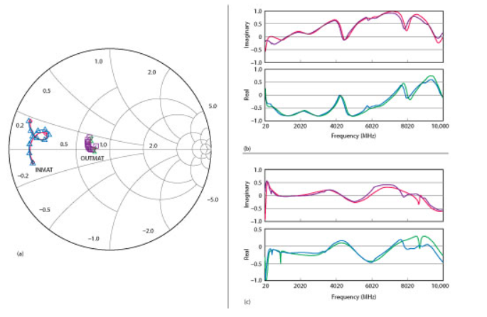
Figure 5 shows the measured versus modeled INMAT and OUTMAT impedances from 1000 to 3000 MHz (a); INMAT (b) and OUTMAT (c) circuit measurements of impedance versus modeled impedance in the 20 MHz to 10 GHz range.
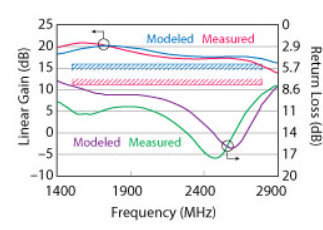
Figure 6 shows the modeled versus measured small signal gain and input return loss.
Passive Measurement
Before completing assembly, the impedances of the INMAT and OUTMAT circuits (presented to the transistor terminals) were measured to correlate the modeled and measured datasets. The measured data shows very good consistency with the un-tuned modeled impedance in the range of 1000 to 3000 MHz (see Figure 5a). Measurements of the INMAT and OUTMAT circuits over a wider bandwidth from 20 MHz to 10 GHz still show very good agreement between modeled and measured impedances (see Figure 5b and 5c). With the modular three-piece fixture, the impedance seen by the device can be accurately measured directly without the use of mechanically cumbersome probes, which would introduce electrical parasitic inductance, particularly stray inductance, at the connection points. The fixture is not a production version of the amplifier, but an important step in the design process to eliminate uncertainty at each design stage.
Small Signal Measurement
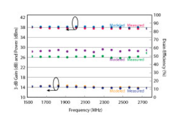
Figure 7 shows the modeled versus measured large signal CW power, gain, and efficiency.
The initial small signal gain measurements used V ds = +28 V and I dq = 90 mA drain bias. The measured and modeled gain and impedance matching correlate closely with greater than 16 dB small signal gain and greater than 7.5 dB input return loss across the operating bandwidth (see Figure 6). The amplifier was stable during actual stability tests (such as varying drain rail voltage and using external tuners to alter the source impedance seen by the device).
Large Signal Measurement
Large signal measurements were taken using V ds = +28 V and I dq = 90 mA drain bias. The amplifier was driven by feeding a continuous wave signal source into the amplifier. RF input and output power measurements were corrected for any compression in the driver. Power gain, drain efficiency, and power delivered to the load were measured at 3 dB compression. The modeled results show a maximum P3dB of 41 dBm, maximum drain efficiency of 63.2%, and maximum gain of 16.4 dB. Measured results show P 3dB of 40.6 dBm, maximum drain efficiency of 59.1%, and maximum gain of 15.7 dB (see Figure 7). The RFPA provides over 10 W of power from as low as 1300 MHz to as high as 2900 MHz, extending its range to 76.2% of the fractional bandwidth.

Figure 8 shows the intermodulation performance of the single-ended amplifier with a 2.5 MHz, 9.5 dB COFDM signal.
To evaluate the efficiency and intermodulation sideband performance in output-backoff mode, a 2.5 MHz channel bandwidth COFDM signal with a 9.5 dB PAPR was used in the 2.0 to 2.5 GHz band. As a single-ended amplifier with an output power of 34.5 dBm, the average efficiency was 34% to 35.9%, with linearity measured at 30 dBc at a center frequency of ±1.25 MHz (see Figure 8). Similar results were obtained using a WCDMA test signal with PAPR = 7.8 dB in the 1.805 to 1.88 GHz band.
A balanced version of the amplifier is under construction. Including imperfect mixing, it is expected to achieve +37 dBm with an average efficiency of about 34%, and linearity of 30 dBc at a center frequency of ±1.25 MHz. Linearization techniques such as digital predistortion or envelope tracking can be used to improve linearity. Achieving high efficiency at peak signal levels allows the amplifier to operate at higher relative power across the entire dynamic range, thus improving efficiency and linearity even with high PAPR signals.
Conclusion
A method for designing broadband, linear, and efficient RFPAs minimizes uncertainty to achieve first-time success. The design method consists of four stages: device selection using qualitative and quantitative analysis, load and source impedance matching network optimization using load and source pulling, passive network synthesis (including EM verification and waveform engineering using intrinsic voltage and current nodes). These techniques together provide a validated systematic approach to designing the entire RFPA.
A measurement technique for manufacturing source and load networks, capable of comparing modeled and measured impedances at the transistor junctions, has also been demonstrated using a three-piece fixture. Passive network synthesis using SRFT techniques combined with the analysis of mismatch loss and transducer power gain provides broadband matching with relatively simple matching networks.
Acknowledgments
The authors would like to thank Andy Wallace from AWR Group, NI, and Qorvo/Modelithics for providing device models.
References
-
DT Wu, F. Mkadem, and S. Boumaiza, “Design of a Broadband and Efficient 45 W GaN Power Amplifier Using Simplified Real Frequency Technique,” IEEE MTT-S International Microwave Symposium, May 2010, pp. 1091-1092.
-
RA Beltran, “Load Network Design for F Class and Inverse F Class Power Amplifiers Based on Transmission Zeros,” IEEE MTT-S International Microwave Symposium, June 2014.
-
PLD Abrie, “Design of RF and Microwave Amplifiers and Oscillators, 1st Edition,” Artech House, 1999.
-
DM Pozar, “Microwave Engineering, 2nd Edition,” Wiley, 1998.
-
SC Cripps, “RF Power Amplifiers for Wireless Communications, 2nd Edition,” Artech House, 2006.