

Micro piezoelectric ultrasonic transducers (pMUTs) have significant applications in fields such as medical imaging, fingerprint recognition, distance detection, and gesture recognition. The emission sensitivity of the device is one of the most important indicators for evaluating the pMUT emitter, in which the piezoelectric layer plays a critical role. In recent years, the piezoelectric layer materials of pMUTs that have received much attention are mainly AlN and PZT-based materials. However, the ferroelectric PZT has a larger piezoelectric coefficient, thus exhibiting superior performance in pMUTs (especially the emitter) compared to non-ferroelectric AlN. Nonetheless, the toxicity of lead in PZT poses risks to human health and the environment, making the development of lead-free ferroelectric film-based pMUTs of great significance. Among various lead-free ferroelectric materials, the K0.5Na0.5NbO3 (KNN) system has piezoelectric properties comparable to PZT and is considered one of the most promising lead-free ferroelectric piezoelectric materials to replace PZT. Currently, mature semiconductor processing techniques are typically applicable to larger films, and there are still significant challenges in preparing large-area, high-quality lead-free ferroelectric films. Therefore, despite extensive research on the structure and properties of lead-free ferroelectric piezoelectric films in recent years, the exploration of their application in pMUT devices remains blank.
Point 1: pMUT Device Fabrication Process
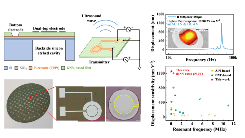
This work successfully fabricated high-quality films with a composition of 0.95(K0.49Na0.49Li0.02)(Nb0.8Ta0.2)O3-0.05CaZrO3-3 mol.% Mn (KNN-LT-CZ5-Mn3) on a 2-inch SOI substrate (Si/SiO2/Si) using a low-cost sol-gel method. Highly integrated pMUT devices were obtained through microfabrication. The specific microfabrication process includes: first, wet etching to create the bottom electrode, followed by photolithography, lift-off, and magnetron sputtering to create the top electrode, and finally using photolithography and deep reactive ion etching (deep-RIE) to form the cavity after back silicon etching, resulting in the pMUT device.
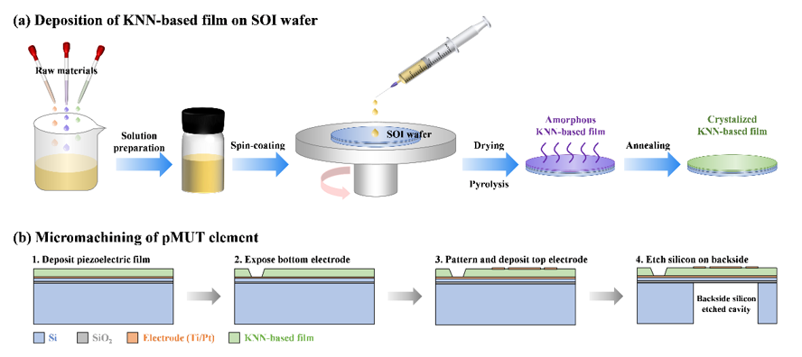
Figure 1 Fabrication Process of pMUT Devices (a) Deposition of KNN-LT-CZ5-Mn3 piezoelectric films on 2-inch SOI wafers via sol-gel method (b) Microfabrication process of pMUT elements
Point 2: Structure Morphology and Electrical Properties of KNN Films
As shown in Figure 2 (a), the KNN films deposited on the 2-inch SOI silicon wafer exhibit a mirror-like shiny characteristic, indicating high film quality; SEM and AFM images further confirm the dense and uniform microstructural features of the films. Additionally, the out-of-plane (001) preferred orientation is clearly reflected through bright field TEM, high-resolution TEM Fourier transform, and XRD results. Notably, the SHG patterns in both horizontal and vertical modes show that the off-region presents double symmetry, consistent with the characteristics of the orthorhombic phase, while the on-region exhibits significant fourfold symmetric components in the vertical mode, indicating the presence of the tetragonal phase. The abnormal shift of the Raman peak position A1g(ν1) near room temperature further indicates the coexistence of O-T phases in the films at room temperature. The material’s good (001) texture and phase coexistence are favorable for achieving high piezoelectric response and excellent emission sensitivity of pMUT devices.
Figure 2 (a) Photo of KNN-LT-CZ5-Mn3 films grown on 2-inch SOI silicon wafers via sol-gel method; (b) Cross-sectional SEM image of the films; (c) Surface AFM image of the films; (d) Cross-sectional TEM image of the films; (e) High-resolution image of a certain area of the cross-section of the films (inset is the Fourier transform image of the selected area); (f) XRD pattern of the films; (g) Enlarged view of the (200) peak; (h) Temperature-dependent Raman spectra of the films; (i) SHG signal distribution map within a 50*50 micron area (on and off represent strong and weak response areas, near represents areas with intermediate response); (j) Testing of SHG polar anisotropy in different regions; (k-l) SHG patterns in the vertical and horizontal modes for strong (on) and weak (off) signal areas
Moreover, from the piezoelectric force microscopy (PFM), it can be observed that the domain sizes in the films are on the order of tens of nanometers and are uniformly randomly distributed, possessing low domain wall energy, which allows for flexible response under an external electric field, aiding in enhancing the piezoelectric response. The SS-PFM amplitude exhibits a nonlinear butterfly curve, indicating the contribution of non-intrinsic effects. The SS-PFM phase curve shows that the films exhibit 180º polarization reversal characteristics, indicating good ferroelectricity of the films. Furthermore, macroscopic electrical performance tests indicate that the films possess low loss and leakage current, and their good insulation performance allows for full polarization, generating greater vibration displacement, laying the foundation for the excellent performance of pMUT devices.
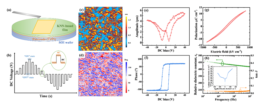
Figure 3 (a) Schematic diagram of the PFM scanning process; (b) Loading curve of the electrical signal during the SS-PFM testing process; (c-d) Amplitude and phase of the out-of-plane PFM; (e-f) Amplitude and phase hysteresis curves of SS-PFM in the OFF state; (g) Hysteresis loop (h) Variation of relative permittivity and loss with frequency, the inset in (h) shows the leakage current curve of the films.
Point 3: Quality and Performance of pMUT Devices
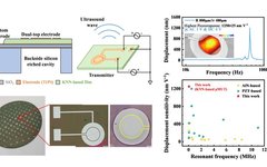
In addition to the quality of the films themselves, the microfabrication process also significantly impacts the performance of pMUT devices. This paper designed pMUT devices of different sizes and shapes, including circular devices with radii of 1000 μm, 800 μm, and 500 μm (corresponding inner electrode radii of 580 μm, 480 μm, and 290 μm) as well as small square devices with a side length of 400 μm (inner electrode side length of 240 μm). As shown in Figures 4 (b) and 4 (d), the designed double top electrode structure and back-etched patterns are well presented, with a minimum linewidth of 20 μm, and the device yield is high, indicating good compatibility between the KNN lead-free films and MEMS processes.

Figure 4 (a) Design of photomask for top electrode pattern; (a1) Circular (a2) Square double top electrodes; (b) Top electrodes of different sizes and shapes obtained through lift-off process, with the inset showing an enlarged view of a single top electrode; (c) Design diagram of back silicon etching patterns (d) Devices obtained after deep reactive ion etching (Deep-RIE) of the back silicon (back view); enlarged views of a single (d1) circular device and (d2) square device.
The emission sensitivity of the device is an important indicator for evaluating the emission performance of pMUTs, which can be described by dynamic displacement sensitivity, i.e., the ratio of vibration displacement at the resonant frequency to the amplitude of the AC driving voltage (in units of nm V-1). The main resonant frequency of devices of different sizes shows significant differences, with a clear pattern observed: as the device size increases, the resonant frequency shifts to lower frequencies, demonstrating the tunability of the device’s operating frequency. Notably, the medium-sized R800 device exhibits a relatively high dynamic displacement sensitivity (~1250 nm V-1) at a resonant frequency of 66.2 kHz, outperforming most PZT/AlN-based pMUTs. Due to the strong penetration of low-frequency signals, which is beneficial for long-distance detection, the KNN-based pMUT devices with high emission sensitivity at low frequencies obtained in this work are expected to play an important role in long-distance detection. Furthermore, when the device size is reduced to a side length of 400 μm, it can be observed that the resonant frequency of the device exceeds 200 kHz, and the dynamic displacement sensitivity (~300 nm V-1) also shows certain advantages compared to AlN.
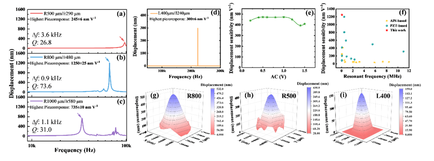
Figure 5 Electromechanical performance of pMUT devices of different sizes and shapes (R1000, R800, R500, and L400) (a-d) Dynamic displacement response of devices of different sizes and shapes under 4V DC and 1V AC test conditions; (e) Displacement sensitivity of R800 device under different AC voltages (keeping 1V DC); (f) Comparison of dynamic displacement sensitivity of KNN-based pMUTs (R800) with PZT and AlN-based pMUTs in this work. (g-h) 3D vibration displacement scanning images of different devices under 2V DC and 1V AC conditions
Finally, this paper analyzes the static displacement sensitivity of KNN-based films before and after back silicon etching. The results show that the high vibration displacement of pMUT devices comes not only from the high piezoelectric response of the films themselves but also from the changes in stress state and vibration mode brought about by back silicon etching. For the films before etching, they are subjected to the clamping effect and stress from the substrate, which suppresses the piezoelectric response of the films; however, after back silicon etching, both the clamping effect and stress from the substrate are released, thereby enhancing the apparent piezoelectric response of the films. More importantly, the vibration mode of the films after back silicon etching changes from the 33 mode to the 31 mode, meaning that applying an electric field in the thickness direction will induce transverse tensile stress (Figure 6d) or compressive stress (Figure 6e) in the in-plane direction of the films, generating a bending moment that forces the films to deform in the out-of-plane direction (d31 mode), resulting in significant bending vibrations in this structure, thus greatly enhancing the displacement sensitivity of the devices.
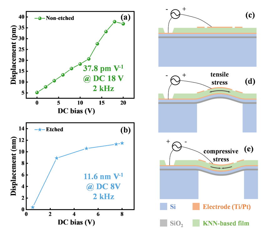
Figure 6 (a) Vibration displacement variation of KNN films before back silicon etching and (b) after back silicon etching under 2kHz 1V AC voltage; (c-e) Comparison of vibration modes of KNN films before and after back silicon etching under applied electric fields
Literature link: https://doi.org/10.1016/j.nanoen.2022.107761
END
The WeChat public account “Dielectrics” sincerely invites readers to submit articles, including but not limited to: recent research achievements, in-depth interpretations of classic articles, introduction of testing principles, analysis of research software, software operation tutorials, introductory tutorials for research, recommendations for related books, sharing of research skills, recommendations for academic conferences and lectures, as well as recruitment and admissions. For more details, please click: Dielectrics – Call for Submissions


If you find this useful, please click here↓↓↓