Skip to content
Translator|Hu Yanjun, Cheng Haoyuan
In recent years, the scale of neural network models has grown exponentially, from BERT with over 100 million parameters in 2018 to GPT-3 with 175 billion parameters in 2020, an increase of three orders of magnitude in just two years, and this growth shows no signs of stopping.
People have just begun to explore the application potential of neural networks, but traditional training and inference methods can no longer keep pace with the rapid growth of neural network scales, failing to meet the memory and computing power requirements needed for large-scale machine learning. To address this challenge, many startups both domestically and internationally are seeking substantial underlying technology innovations in hardware and software.
As an AI accelerator startup that has garnered significant attention in the industry, Cerebras, founded in 2016, aims to solve AI computing problems by building a brand new AI accelerator solution to achieve orders of magnitude in computational performance: First, it is necessary to improve the computing core architecture, rather than merely increasing the floating-point operations per second; second, the chip integration density must be increased at a rate exceeding Moore’s Law; finally, cluster connections should be simplified to greatly enhance cluster computing efficiency.
To achieve the above goals, Cerebras has designed a new computing core architecture. This architecture allows a single device to run ultra-large-scale models. Additionally, it has developed horizontal scaling and local unstructured sparse acceleration technologies that only require simple data parallelism, significantly lowering the barriers to the application of large models.
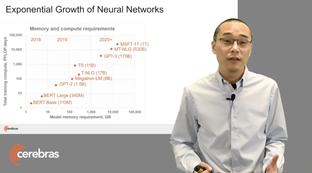 Figure 1: Memory and computational requirements of various SOTA neural network models in recent years
In 2021, Cerebras launched the world’s largest AI chip, the Wafer Scale Engine 2 (WSE-2), which has an area of 46,225 square millimeters, is built using a 7nm process, contains 2.6 trillion transistors, and 850,000 AI-optimized cores. It also introduced the world’s first human brain-scale AI solution, the CS-2 AI computer, capable of supporting training scales of over 120 trillion parameters. In June of this year, it trained the world’s largest NLP model with 20 billion parameters on the CS-2 system based on a single WSE-2 chip, significantly reducing the cost that would have originally required thousands of GPUs for training.
At the recent Hot Chips conference, Cerebras co-founder and chief hardware architect Sean Lie provided an in-depth introduction to Cerebras hardware, showcasing their innovative approaches in core architecture, vertical scaling, and horizontal scaling. Below are the highlights of his presentation, compiled by the OneFlow community.
Figure 1: Memory and computational requirements of various SOTA neural network models in recent years
In 2021, Cerebras launched the world’s largest AI chip, the Wafer Scale Engine 2 (WSE-2), which has an area of 46,225 square millimeters, is built using a 7nm process, contains 2.6 trillion transistors, and 850,000 AI-optimized cores. It also introduced the world’s first human brain-scale AI solution, the CS-2 AI computer, capable of supporting training scales of over 120 trillion parameters. In June of this year, it trained the world’s largest NLP model with 20 billion parameters on the CS-2 system based on a single WSE-2 chip, significantly reducing the cost that would have originally required thousands of GPUs for training.
At the recent Hot Chips conference, Cerebras co-founder and chief hardware architect Sean Lie provided an in-depth introduction to Cerebras hardware, showcasing their innovative approaches in core architecture, vertical scaling, and horizontal scaling. Below are the highlights of his presentation, compiled by the OneFlow community.
Cerebras Computing Core Architecture
The compute core is the “heart” of all computer architectures, and Cerebras has redesigned the compute core for the fine-grained dynamic sparsity of neural networks.
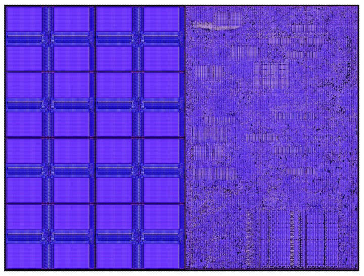 Figure 2: Cerebras Compute Core
Figure 2 shows a small core that measures only 38,000 square micrometers, half of which is silicon area dedicated to 48 KB of memory, while the other half contains 110,000 standard cells of computational logic. The entire compute core operates efficiently at a clock frequency of 1.1 GHz, with a peak power consumption of only 30 milliwatts.
Let’s start with memory. Traditional architectures like GPUs use shared central DRAM, but DRAM access speeds are slow and located far away. Even with cutting-edge technologies like interposers and HBM, their memory bandwidth still falls far short of the core data path bandwidth. For instance, the data path bandwidth is typically 100 times that of memory bandwidth.
This means that every operand coming from memory must be used at least 100 times in the data path to achieve high utilization. Traditionally, this has been addressed through local caching and local registers to achieve data reuse.
However, there is a method to allow the data path to utilize memory bandwidth at peak performance: by placing memory completely adjacent to the units that will use it. This way, memory bandwidth equals the operand bandwidth of the core data path.
This is a simple physical principle: moving bit data from local memory to the data path requires only a few tens of micrometers, which is much easier than transferring it through packaging connectors, PCBs, or cables.
Figure 2: Cerebras Compute Core
Figure 2 shows a small core that measures only 38,000 square micrometers, half of which is silicon area dedicated to 48 KB of memory, while the other half contains 110,000 standard cells of computational logic. The entire compute core operates efficiently at a clock frequency of 1.1 GHz, with a peak power consumption of only 30 milliwatts.
Let’s start with memory. Traditional architectures like GPUs use shared central DRAM, but DRAM access speeds are slow and located far away. Even with cutting-edge technologies like interposers and HBM, their memory bandwidth still falls far short of the core data path bandwidth. For instance, the data path bandwidth is typically 100 times that of memory bandwidth.
This means that every operand coming from memory must be used at least 100 times in the data path to achieve high utilization. Traditionally, this has been addressed through local caching and local registers to achieve data reuse.
However, there is a method to allow the data path to utilize memory bandwidth at peak performance: by placing memory completely adjacent to the units that will use it. This way, memory bandwidth equals the operand bandwidth of the core data path.
This is a simple physical principle: moving bit data from local memory to the data path requires only a few tens of micrometers, which is much easier than transferring it through packaging connectors, PCBs, or cables.
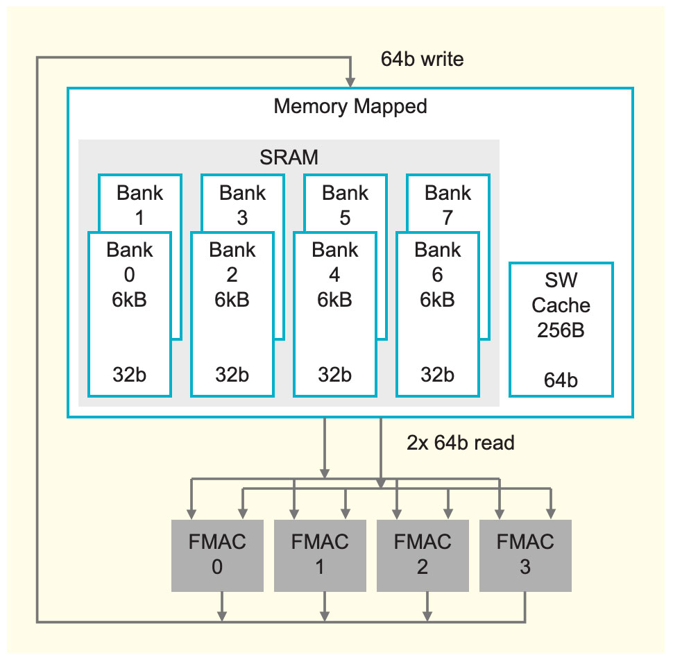 Figure 3: Memory Design of Cerebras Compute Core: Each Core is Equipped with Independent Memory.
Figure 3 illustrates the memory design of the Cerebras compute core, where each core is equipped with 48 KB of local SRAM, featuring eight 32-bit wide single-port banks that provide high density while ensuring optimal performance. This level of bank can provide memory bandwidth far exceeding that required by the data path.
Therefore, we can provide extreme data path performance from memory, requiring only two 64-bit reads and one 64-bit write per cycle, ensuring maximum data path performance. Notably, the memory of each core is independent, with no shared memory in the traditional sense.
In addition to high-performance SRAM, the Cerebras compute core also features a 256-byte software-managed cache for frequently accessed data structures, such as accumulators. This cache is positioned very close to the data path, consuming very little power. The distributed memory architecture described above results in an astonishing memory bandwidth equivalent to 200 times that of GPU memory bandwidth for the same area.
Figure 3: Memory Design of Cerebras Compute Core: Each Core is Equipped with Independent Memory.
Figure 3 illustrates the memory design of the Cerebras compute core, where each core is equipped with 48 KB of local SRAM, featuring eight 32-bit wide single-port banks that provide high density while ensuring optimal performance. This level of bank can provide memory bandwidth far exceeding that required by the data path.
Therefore, we can provide extreme data path performance from memory, requiring only two 64-bit reads and one 64-bit write per cycle, ensuring maximum data path performance. Notably, the memory of each core is independent, with no shared memory in the traditional sense.
In addition to high-performance SRAM, the Cerebras compute core also features a 256-byte software-managed cache for frequently accessed data structures, such as accumulators. This cache is positioned very close to the data path, consuming very little power. The distributed memory architecture described above results in an astonishing memory bandwidth equivalent to 200 times that of GPU memory bandwidth for the same area.
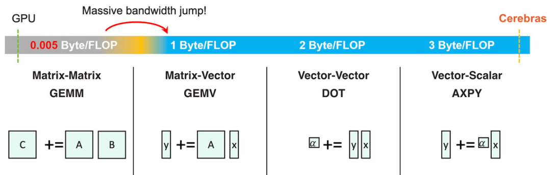
Extreme Performance Across All BLAS Levels
Figure 4: Sparse GEMM executes one AXPY operation for each non-zero weight.
With immense memory bandwidth, many outstanding functions can be achieved. For instance, it can fully leverage the extreme performance across all BLAS levels (Basic Linear Algebra Subprograms, BLAS levels). Traditional CPU and GPU architectures have limited on-chip memory bandwidth, thus can only achieve extreme performance for GEMM (General Matrix Multiplication), which is matrix-matrix multiplication.
As seen in Figure 4, any BLAS level below matrix-matrix multiplication requires a significant increase in memory bandwidth, which traditional architectures cannot satisfy.
However, with sufficient memory bandwidth, GEMV (matrix-vector multiplication), DOT (vector-vector multiplication), and AXPY (vector-scalar multiplication) can all achieve peak performance. High memory bandwidth is particularly important in neural network computations, as it allows for sufficient acceleration of unstructured sparsity. A sparse GEMM operation can be viewed as a collection of multiple AXPY operations (executing once for each non-zero element).
The foundation of the Cerebras compute core is a fully programmable processor, adaptable to the ever-changing demands of deep learning. Like general-purpose processors, the Cerebras core processor supports a variety of instructions such as arithmetic, logic, load/store, comparison, and branching. These instructions, like data, are stored in the 48 KB local memory of each core, meaning that the cores are independent of each other, and the entire chip can perform fine-grained dynamic computation. General-purpose instructions operate on 16 general-purpose registers in a compact six-stage pipeline.
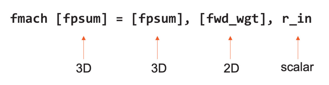 Equation 1, Example of FMAC Instruction
Moreover, the Cerebras core also supports all tensor instructions related to data processing at the hardware level. These tensor operators execute in a 64-bit data path, consisting of four FP16 FMAC (Fused Multiply-Add) units.
To enhance performance and flexibility, the instruction set architecture (ISA) of Cerebras treats tensors as first-class operands, just like general registers and memory. The above Equation 1 is an example of an FMAC instruction, which operates directly on 3D and 2D tensors as operands.
This is made possible because the Cerebras core uses Data Structure Registers (DSR) as operands for instructions. The Cerebras core has 44 DSRs, each containing a descriptor with pointers to tensors and their lengths, shapes, sizes, etc.
With DSRs, the hardware architecture of the Cerebras core is more flexible, allowing support for 4D tensors in memory, as well as fabric streaming tensors, FIFOs (First-In-First-Out), and circular buffers. Additionally, the Cerebras core is equipped with a hardware state machine to manage the flow order of entire tensors through the data path.
Equation 1, Example of FMAC Instruction
Moreover, the Cerebras core also supports all tensor instructions related to data processing at the hardware level. These tensor operators execute in a 64-bit data path, consisting of four FP16 FMAC (Fused Multiply-Add) units.
To enhance performance and flexibility, the instruction set architecture (ISA) of Cerebras treats tensors as first-class operands, just like general registers and memory. The above Equation 1 is an example of an FMAC instruction, which operates directly on 3D and 2D tensors as operands.
This is made possible because the Cerebras core uses Data Structure Registers (DSR) as operands for instructions. The Cerebras core has 44 DSRs, each containing a descriptor with pointers to tensors and their lengths, shapes, sizes, etc.
With DSRs, the hardware architecture of the Cerebras core is more flexible, allowing support for 4D tensors in memory, as well as fabric streaming tensors, FIFOs (First-In-First-Out), and circular buffers. Additionally, the Cerebras core is equipped with a hardware state machine to manage the flow order of entire tensors through the data path.
Fine-Grained Data Flow Scheduling
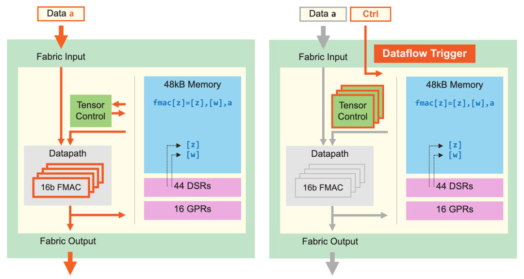 Figure 5: Core Data Path and Core Data Flow Scheduling. Fine-Grained Dynamic Computing Cores Can Enhance Computational Performance, Sparsity Utilization is 10 Times That of GPUs.
In addition to improving tensor applications, the Cerebras core can also execute fine-grained data flow scheduling. As shown in Figure 5, all computations are triggered by data. Fabric directly transmits data and associated controls in hardware; once the core receives data, it begins to look up execution instructions based entirely on the received data. This data flow mechanism transforms the entire computation structure into a data flow engine, capable of supporting sparse acceleration—since it only processes non-zero data. The sender filters out all zero values, so the receiver only receives non-zero values, and all computations are triggered by non-zero data.
This approach not only conserves power but also eliminates unnecessary computations, enhancing computational efficiency. Operations are triggered by individual data elements, allowing the Cerebras core to support ultra-fine-grained, fully unstructured sparsity without performance loss. Due to the dynamic nature of data flow, the Cerebras core also supports the simultaneous operation of eight tensor operations, which we call “micro-threads.”
Micro-threads are independent of each other, allowing hardware to switch between them during each cycle. The scheduler continuously monitors the availability of inputs and outputs for all tensors awaiting processing and incorporates a priority processing mechanism to ensure that critical tasks are prioritized. When switching between different tasks generates significant dynamic behavior, micro-threads can enhance utilization; otherwise, these dynamic behaviors may cause pipeline bubbles.
The aforementioned characteristics of fine-grained, dynamic, and small core architecture provide our architecture with unprecedented high performance, with unstructured sparse computing utilization at least 10 times that of GPUs. It is evident that through improvements to the compute core architecture, Cerebras can achieve orders of magnitude in performance enhancement.
Figure 5: Core Data Path and Core Data Flow Scheduling. Fine-Grained Dynamic Computing Cores Can Enhance Computational Performance, Sparsity Utilization is 10 Times That of GPUs.
In addition to improving tensor applications, the Cerebras core can also execute fine-grained data flow scheduling. As shown in Figure 5, all computations are triggered by data. Fabric directly transmits data and associated controls in hardware; once the core receives data, it begins to look up execution instructions based entirely on the received data. This data flow mechanism transforms the entire computation structure into a data flow engine, capable of supporting sparse acceleration—since it only processes non-zero data. The sender filters out all zero values, so the receiver only receives non-zero values, and all computations are triggered by non-zero data.
This approach not only conserves power but also eliminates unnecessary computations, enhancing computational efficiency. Operations are triggered by individual data elements, allowing the Cerebras core to support ultra-fine-grained, fully unstructured sparsity without performance loss. Due to the dynamic nature of data flow, the Cerebras core also supports the simultaneous operation of eight tensor operations, which we call “micro-threads.”
Micro-threads are independent of each other, allowing hardware to switch between them during each cycle. The scheduler continuously monitors the availability of inputs and outputs for all tensors awaiting processing and incorporates a priority processing mechanism to ensure that critical tasks are prioritized. When switching between different tasks generates significant dynamic behavior, micro-threads can enhance utilization; otherwise, these dynamic behaviors may cause pipeline bubbles.
The aforementioned characteristics of fine-grained, dynamic, and small core architecture provide our architecture with unprecedented high performance, with unstructured sparse computing utilization at least 10 times that of GPUs. It is evident that through improvements to the compute core architecture, Cerebras can achieve orders of magnitude in performance enhancement.
Vertical Scaling: Beyond Moore’s Law
To vertically scale chips, traditional methods focus on chip manufacturing, namely increasing chip integration density. Over the past few decades, the development of the chip industry has adhered to Moore’s Law, with increasing chip integration density. Today, Moore’s Law continues, but its increments are not large enough, with each generation of process only able to double the integration density, which is insufficient to meet the computational demands of neural networks. Therefore, Cerebras aims to exceed Moore’s Law to achieve orders of magnitude in performance improvement.
To this end, we have tried traditional methods—expanding chip area—and have achieved extreme results, culminating in the WSE-2 (Wafer-Scale Engine). Today, the WSE-2 is widely applied. It is the largest chip in the world, measuring over 46,000 square millimeters, 56 times the size of the largest CPU currently available. A single WSE-2 contains 2.6 trillion transistors and has 850,000 cores. The enormous chip area enables vast on-chip memory and extremely high performance.
To ensure that the impressively sized WSE-2 can be used in standard data center environments, we have also specifically designed the Cerebras CS-2 system to achieve cluster-level computation with a single chip.
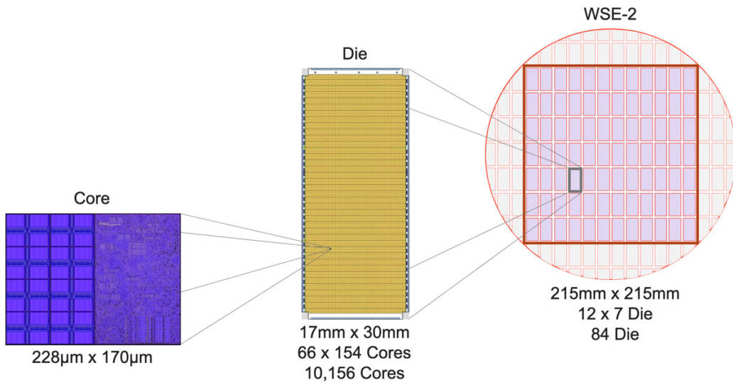
Figure 6: From Small Cores to Large Wafer-Scale Engines
The following describes our process of building a large wafer-scale engine from small cores: First, we create traditional dies on a wafer with a diameter of about 300 millimeters, each containing about 10,000 cores; then, unlike in the past, we do not cut out individual dies to create traditional chips, but instead cut out a square with a side length of 215 millimeters from the entire wafer, which contains 84 dies, totaling 850,000 computing cores (Figure 6).
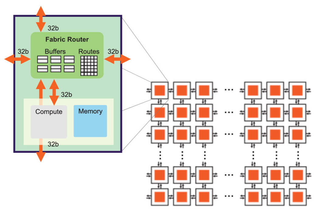 Figure 7: High Bandwidth, Low Latency Chip Structure
Achieving such an enormous chip size relies on the cooperation of the underlying architecture, which must enable efficient and high-performance data transfer across the entire wafer (Figure 7). The Cerebras chip structure employs a 2D mesh topology, which is highly suitable for scaling and incurs very low overhead.
The mesh topology connects all cores, with each core having a structural router (fabric router). Each structural router has five ports, one in each direction and one facing the core itself, with each port having a 32-bit bidirectional interface. The advantage of having fewer ports is that it keeps inter-node latency within a single clock cycle, enabling low-cost, lossless flow control with very low buffering.
The basic data packets in the chip are single FP16 data elements optimized for neural networks, accompanied by 16-bit control information, forming 32-bit ultra-fine-grained data packets.
To further optimize the chip structure, we use static routing, which is efficient, low-cost, and can fully utilize the static connections of neural networks. To allow multiple routes on the same physical connection, we provide 24 independent static routes for configuration, which are non-blocking and can all be transmitted over the same physical connection using time-multiplexing technology.
Finally, due to the high fan-out required for neural network transmission, each structural router in the Cerebras chip has native broadcast and multicast capabilities.
With the above foundation in place, we can proceed with scaling. Scaling within a single die is relatively simple, but now we need to connect dies to each other. To cross the scribe lines (less than a millimeter wide) between dies, we use advanced metal layers from TSMC technology.
We extend the computing cores into a 2D mesh computing structure and then form a completely homogeneous array of computing cores across the entire wafer. The die-die interface is an efficient source-synchronous parallel interface; however, on such a large wafer scale, there are over a million lines, so our underlying protocol must employ redundancy design. We achieve this through training and automatic correction state machines. With these interfaces, even if there are defects during manufacturing, the entire wafer structure can maintain a uniform fabric.
Figure 8: Homogeneous Structure Across the Entire Wafer.
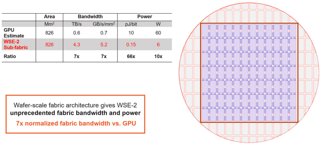
The seemingly simple short lines on the chip are actually very important; their distance on silicon is less than a millimeter. This line design is very different from traditional SERDES methods. Like the previously mentioned memory design, the short line design is based on a simple physical principle: transmitting bit data across less than 1 millimeter on the chip is much easier than transmitting through packaging connectors, PCBs, or cables.
This method brings orders of magnitude improvements compared to traditional IO. As shown in the data of Figure 8, the WSE-2 has about an order of magnitude more bandwidth per unit area than GPUs, and its power efficiency per bit has improved by nearly two orders of magnitude. All these indicate that the entire wafer structure possesses unprecedented high performance.
When converted to the equivalent GPU area, the bandwidth of the WSE-2 is seven times that of GPUs, while the power consumption is only about 5 watts. It is this level of global structural performance that allows the wafer to operate as a single chip. With such a powerful single chip, we can tackle some extremely challenging problems.
Figure 7: High Bandwidth, Low Latency Chip Structure
Achieving such an enormous chip size relies on the cooperation of the underlying architecture, which must enable efficient and high-performance data transfer across the entire wafer (Figure 7). The Cerebras chip structure employs a 2D mesh topology, which is highly suitable for scaling and incurs very low overhead.
The mesh topology connects all cores, with each core having a structural router (fabric router). Each structural router has five ports, one in each direction and one facing the core itself, with each port having a 32-bit bidirectional interface. The advantage of having fewer ports is that it keeps inter-node latency within a single clock cycle, enabling low-cost, lossless flow control with very low buffering.
The basic data packets in the chip are single FP16 data elements optimized for neural networks, accompanied by 16-bit control information, forming 32-bit ultra-fine-grained data packets.
To further optimize the chip structure, we use static routing, which is efficient, low-cost, and can fully utilize the static connections of neural networks. To allow multiple routes on the same physical connection, we provide 24 independent static routes for configuration, which are non-blocking and can all be transmitted over the same physical connection using time-multiplexing technology.
Finally, due to the high fan-out required for neural network transmission, each structural router in the Cerebras chip has native broadcast and multicast capabilities.
With the above foundation in place, we can proceed with scaling. Scaling within a single die is relatively simple, but now we need to connect dies to each other. To cross the scribe lines (less than a millimeter wide) between dies, we use advanced metal layers from TSMC technology.
We extend the computing cores into a 2D mesh computing structure and then form a completely homogeneous array of computing cores across the entire wafer. The die-die interface is an efficient source-synchronous parallel interface; however, on such a large wafer scale, there are over a million lines, so our underlying protocol must employ redundancy design. We achieve this through training and automatic correction state machines. With these interfaces, even if there are defects during manufacturing, the entire wafer structure can maintain a uniform fabric.
Figure 8: Homogeneous Structure Across the Entire Wafer.
The seemingly simple short lines on the chip are actually very important; their distance on silicon is less than a millimeter. This line design is very different from traditional SERDES methods. Like the previously mentioned memory design, the short line design is based on a simple physical principle: transmitting bit data across less than 1 millimeter on the chip is much easier than transmitting through packaging connectors, PCBs, or cables.
This method brings orders of magnitude improvements compared to traditional IO. As shown in the data of Figure 8, the WSE-2 has about an order of magnitude more bandwidth per unit area than GPUs, and its power efficiency per bit has improved by nearly two orders of magnitude. All these indicate that the entire wafer structure possesses unprecedented high performance.
When converted to the equivalent GPU area, the bandwidth of the WSE-2 is seven times that of GPUs, while the power consumption is only about 5 watts. It is this level of global structural performance that allows the wafer to operate as a single chip. With such a powerful single chip, we can tackle some extremely challenging problems.
Supporting Ultra-Large Models Through Weight Streaming Technology
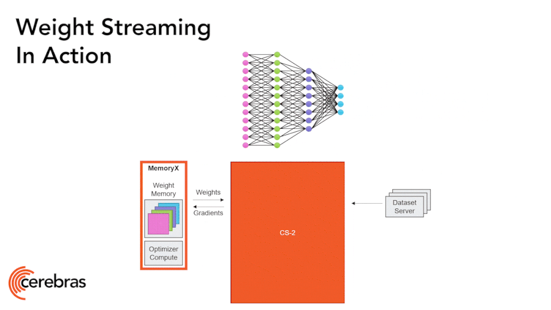
Figure 9: Weight Streaming Technology Supports All Model Sizes on a Single Chip.
The high-performance chip structure allows us to run large neural networks on a single chip. The WSE-2 has sufficient performance and capacity to run today’s largest models without partitioning or complex distributed processing, achieved by decomposing neural network models, weights, and computations.
We store all model weights in an external device called MemoryX and stream these weights to the CS-2 system. The weights are utilized in the computations of each layer of the neural network, with only one layer computed at a time. The weights are not stored in the CS-2 system, not even temporarily. Once the CS-2 receives the weights, it executes computations using the underlying data flow mechanism within the core (Figure 9).
Each individual weight triggers a computation as a separate AXPY operation. After the computation is completed, the weight is discarded, and the hardware proceeds to process the next element. Since the chip does not need to store weights, the memory capacity of the chip does not affect the size of the model it can handle. During backpropagation, gradients flow back to the MemoryX unit in the opposite direction, where the MemoryX unit performs weight updates.
Figure 10: The Complete Wafer is a MatMul Array, Supporting Ultra-Large Matrices.
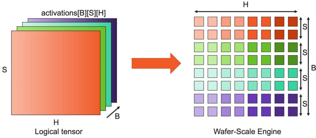
The following describes how computations are executed in the chip. The computations of each layer of the neural network can be reduced to matrix multiplication; due to the large scale of the CS-2, we can utilize the 850,000 cores of the wafer as a single giant matrix multiplier.
It works like this: for transformer models like GPT, the activation tensor has three logical dimensions: batch (B), sequence (S), and hidden (H) dimensions. We split these tensor dimensions across the two-dimensional core mesh on the wafer. The hidden dimension is split in the x-direction of the chip structure, while the batch and sequence dimensions are split in the y-direction. This allows for efficient weight broadcasting and efficient reduction of the sequence and hidden dimensions.
The activation functions are stored on the cores responsible for executing the computations, and the next step is to trigger the computations of these activation functions, accomplished by using on-chip broadcast structures to send weights, data, and commands to each column.
Of course, under the hardware data flow mechanism, weights directly trigger FMAC operations. These are AXPY operations. Since broadcasting occurs at the column level, all cores containing the same feature subset receive the same weights. Additionally, we send commands to trigger other computations, such as reductions or nonlinear operations.
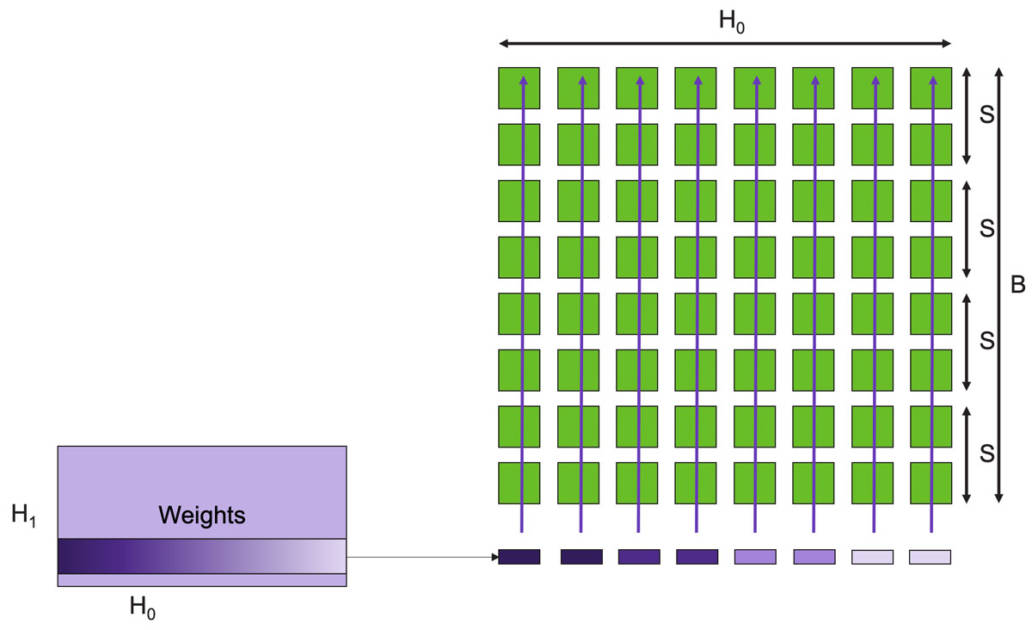 Figure 11: Data Flow Scheduling Achieves Fully Unstructured Sparse MatMul Operations with Low Overhead.
For example, we first broadcast the weight rows across the entire wafer (Figure 11). Each element of each row is a scalar, and of course, within a single row, multiple weights are mapped to a single column. When sparsity is present, only non-zero weights are broadcast to the column, triggering FMAC computations. We skip all zero weights and input the next non-zero weight, which is the reason for achieving sparse acceleration.
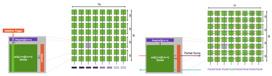
Figure 12: Sparse Input GEMM: Multiplication and Partial Sum Reduction.
If we now zoom in on a core, we can see how the core architecture performs this operation (Figure 12). Under the data flow mechanism, once the weights arrive, they trigger FMAC computations on the core. The weight values are multiplied by each activation function output and then accumulated into the local accumulator in the software-managed cache. FMAC computations are executed using tensor instructions, treating activation function outputs as tensor operands. None of the above computations impose additional overhead on the core.
Moreover, weights do not incur memory overhead because once the computation is completed, the core moves on to compute the next weight without needing to store any weights. If the entire row of cores receives weights, each core will generate a partial sum, and then all partial sums from that row of cores will be reduced.
The reduction computation is triggered by command packets broadcast to all cores in each column. Similarly, under the data flow scheduling mechanism, once a core receives a command packet, it triggers the partial sum reduction computation. The actual reduction computation is completed using the core’s tensor instructions, utilizing structured tensor operands. All columns receive a PSUM command. However, one column will receive a special FSUM command, instructing the core to store the final sum. This is done to prepare the output features for the next layer of computation, using the same distribution as the input features.
Upon receiving the command, the core communicates using a structured ring pattern, which is set up using structured static routing. Using micro-threads, all reductions overlap with the FMAC computations of the next weight row, which begin in parallel. Once all weight rows have been processed, the complete GEMM operation is finished, and all activation function outputs are ready for the next layer of computation.
The design outlined above enables various scales of neural networks to run at high performance on a single chip. The unique core memory and chip architecture allow the chip to support ultra-large matrices without the need for partitioning or segmentation, even ultra-large models with up to 100,000 x 100,000 MatMul layers can run without splitting matrices.
If a single WSE-2 chip runs this model, the FP16 sparse performance can reach 75 PetaFLOPS (with higher sparsity, performance can be even greater), and the FP16 dense performance can reach 7.5 PetaFLOPS. This represents our second approach to addressing the challenges of machine learning hardware, achieving another order of magnitude in performance improvement through scaling.
Figure 11: Data Flow Scheduling Achieves Fully Unstructured Sparse MatMul Operations with Low Overhead.
For example, we first broadcast the weight rows across the entire wafer (Figure 11). Each element of each row is a scalar, and of course, within a single row, multiple weights are mapped to a single column. When sparsity is present, only non-zero weights are broadcast to the column, triggering FMAC computations. We skip all zero weights and input the next non-zero weight, which is the reason for achieving sparse acceleration.
Figure 12: Sparse Input GEMM: Multiplication and Partial Sum Reduction.
If we now zoom in on a core, we can see how the core architecture performs this operation (Figure 12). Under the data flow mechanism, once the weights arrive, they trigger FMAC computations on the core. The weight values are multiplied by each activation function output and then accumulated into the local accumulator in the software-managed cache. FMAC computations are executed using tensor instructions, treating activation function outputs as tensor operands. None of the above computations impose additional overhead on the core.
Moreover, weights do not incur memory overhead because once the computation is completed, the core moves on to compute the next weight without needing to store any weights. If the entire row of cores receives weights, each core will generate a partial sum, and then all partial sums from that row of cores will be reduced.
The reduction computation is triggered by command packets broadcast to all cores in each column. Similarly, under the data flow scheduling mechanism, once a core receives a command packet, it triggers the partial sum reduction computation. The actual reduction computation is completed using the core’s tensor instructions, utilizing structured tensor operands. All columns receive a PSUM command. However, one column will receive a special FSUM command, instructing the core to store the final sum. This is done to prepare the output features for the next layer of computation, using the same distribution as the input features.
Upon receiving the command, the core communicates using a structured ring pattern, which is set up using structured static routing. Using micro-threads, all reductions overlap with the FMAC computations of the next weight row, which begin in parallel. Once all weight rows have been processed, the complete GEMM operation is finished, and all activation function outputs are ready for the next layer of computation.
The design outlined above enables various scales of neural networks to run at high performance on a single chip. The unique core memory and chip architecture allow the chip to support ultra-large matrices without the need for partitioning or segmentation, even ultra-large models with up to 100,000 x 100,000 MatMul layers can run without splitting matrices.
If a single WSE-2 chip runs this model, the FP16 sparse performance can reach 75 PetaFLOPS (with higher sparsity, performance can be even greater), and the FP16 dense performance can reach 7.5 PetaFLOPS. This represents our second approach to addressing the challenges of machine learning hardware, achieving another order of magnitude in performance improvement through scaling.
Horizontal Scaling: Why Is It So Difficult
The final aspect is cluster horizontal scaling. Cluster solutions already exist today, but why is horizontal scaling still so challenging?
Figure 13: The Complexity of Distribution Increases Significantly with Cluster Size.
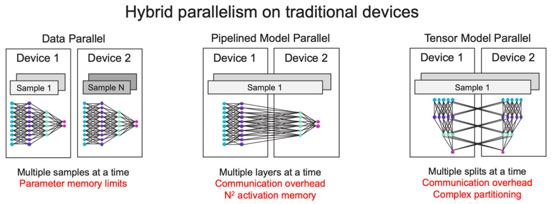
Let’s take a look at existing horizontal scaling technologies (Figure 13). The most common is data parallelism, which is also the simplest method, but it is not suitable for large models because it requires each device to have enough capacity to hold the entire model.
To address this issue, a common approach is to use model parallelism, dividing the model to run different layers of the model in a pipelined manner on different devices. However, as the pipeline lengthens, the activation memory grows at a quadratic rate.
To avoid this, another common model parallelism method is to partition layers across devices, but this incurs significant communication overhead, and partitioning a single layer is very complex.
Due to these limitations, there is still no universal method to achieve horizontal scaling today. In most cases, training massive models requires a mixed approach of data and model parallelism. Existing horizontal scaling solutions still have many shortcomings, with the fundamental reason being simple: in traditional horizontal scaling, memory and computation are tightly coupled, and if a single model runs across thousands of devices, scaling memory and computation becomes a mutually dependent distributed constraint problem.
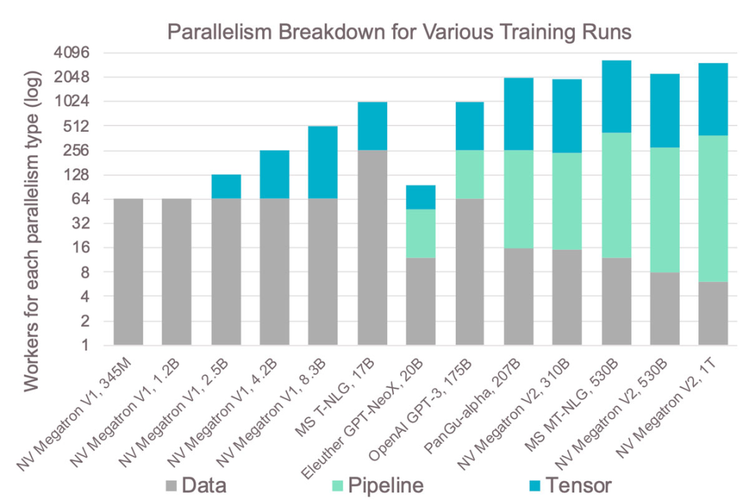
Figure 14: The Complexity of GPU Clusters in Practice.
This complexity leads to results as shown in Figure 14, which displays the largest models trained on GPUs over the past few years and the different parallel methods used. It is evident that larger models require more types of parallelism, increasing complexity.
For instance, the level of parallelism for tensor models is always limited to 8, as there are typically only 8 GPUs in a single server. Therefore, large models often adopt pipelined model parallelism, which is the most complex method due to the aforementioned memory issues. Training models on GPU clusters requires addressing these distributed system issues. This complexity leads to longer development times and often does not achieve optimal scaling.
Cerebras Architecture Makes Scaling Easy
The Cerebras architecture can run all models on a single chip without the need for model partitioning, making scaling simple and natural, allowing for scaling solely through data parallelism without any complex model parallel divisions.
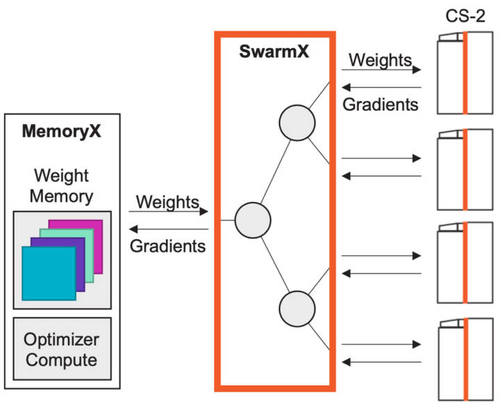 Figure 15: Scaling with MemoryX and SwarmX, Only Near-Linear Data Parallelism is Required.
We have specifically designed the SwarmX interconnect technology for data parallelism. It sits between the MemoryX unit that stores weights and the CS-2 system used for computation, yet is independent of both.
SwarmX broadcasts weights to all CS-2 systems and reduces gradients for all CS-2s; it is not just an interconnect but an active component in the training process, built specifically for data parallel horizontal scaling.
Internally, SwarmX uses a tree topology to achieve modular and low-overhead scaling; being modular and decomposable, it can scale to any number of CS-2 systems with the same execution model as a single system. To scale to more computing power, simply add more nodes and more CS-2 systems to the SwarmX topology. This is our final approach to addressing the demands of machine learning hardware: improving and greatly simplifying horizontal scaling.
Figure 15: Scaling with MemoryX and SwarmX, Only Near-Linear Data Parallelism is Required.
We have specifically designed the SwarmX interconnect technology for data parallelism. It sits between the MemoryX unit that stores weights and the CS-2 system used for computation, yet is independent of both.
SwarmX broadcasts weights to all CS-2 systems and reduces gradients for all CS-2s; it is not just an interconnect but an active component in the training process, built specifically for data parallel horizontal scaling.
Internally, SwarmX uses a tree topology to achieve modular and low-overhead scaling; being modular and decomposable, it can scale to any number of CS-2 systems with the same execution model as a single system. To scale to more computing power, simply add more nodes and more CS-2 systems to the SwarmX topology. This is our final approach to addressing the demands of machine learning hardware: improving and greatly simplifying horizontal scaling.
In recent years, the demand for machine learning workloads has increased by more than three orders of magnitude, with no signs of slowing down. It is expected to grow to the arrow position in Figure 16 in a few years, and we ask ourselves, can we meet this demand?
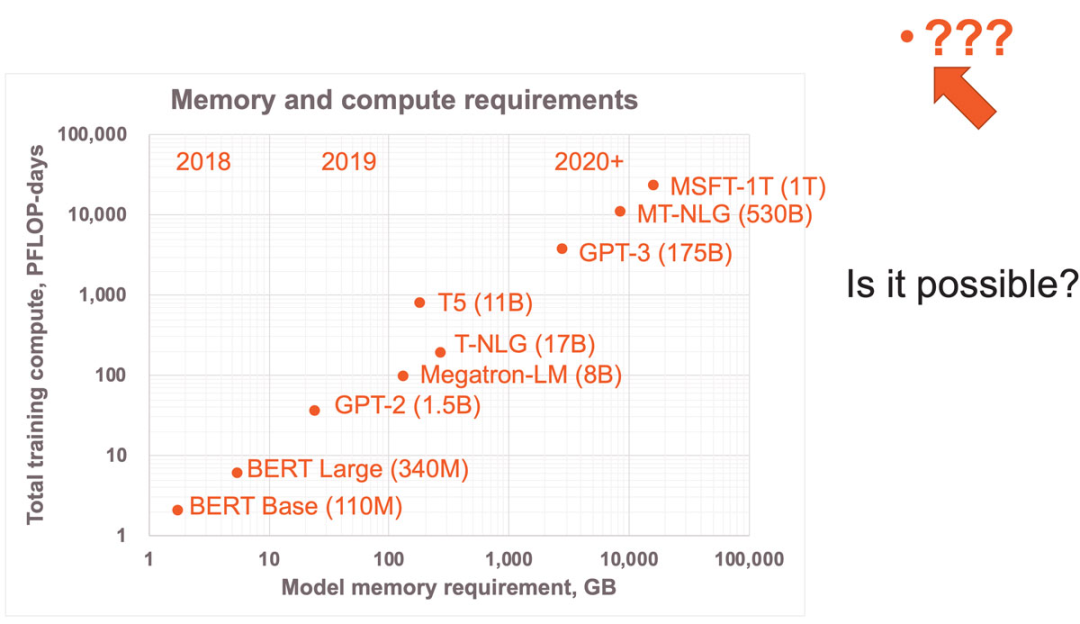 Figure 16: Memory and computation requirements of various state-of-the-art neural networks. Each grid in the horizontal and vertical axes represents an order of magnitude increase.
Cerebras believes we can, but not through traditional technologies, rather through the combination of unstructured sparse acceleration, wafer-scale chips, and cluster horizontal scaling to achieve a threefold increase in performance. The scale of neural network models continues to grow exponentially, and there are few companies that can utilize these large models, and in the future, there will be even fewer.
However, the Cerebras architecture supports running ultra-large models on a single device while enabling horizontal scaling that requires only data parallelism and local unstructured sparse acceleration, allowing more people to utilize large models.
(Original text: https://www.cerebras.net/blog/cerebras-architecture-deep-dive-first-look-inside-the-hw/sw-co-design-for-deep-learning; Video: https://www.youtube.com/watch?v=8i1_Ru5siXc)
Figure 16: Memory and computation requirements of various state-of-the-art neural networks. Each grid in the horizontal and vertical axes represents an order of magnitude increase.
Cerebras believes we can, but not through traditional technologies, rather through the combination of unstructured sparse acceleration, wafer-scale chips, and cluster horizontal scaling to achieve a threefold increase in performance. The scale of neural network models continues to grow exponentially, and there are few companies that can utilize these large models, and in the future, there will be even fewer.
However, the Cerebras architecture supports running ultra-large models on a single device while enabling horizontal scaling that requires only data parallelism and local unstructured sparse acceleration, allowing more people to utilize large models.
(Original text: https://www.cerebras.net/blog/cerebras-architecture-deep-dive-first-look-inside-the-hw/sw-co-design-for-deep-learning; Video: https://www.youtube.com/watch?v=8i1_Ru5siXc)
-
OneFlow v0.8.0 Official Release
-
The Past, Present, and Future of Deep Learning Hardware
-
Winning the Algorithm Competition at Beihang University, Champion Reveals Strategies
-
Groq: Designing a Tensor Streaming Processor Architecture from Scratch
-
Jeff Dean: The Potential of Machine Learning in Hardware Design
-
OneEmbedding: Training TB-Level Recommendation Models on a Single Card is Not a Dream
-
Is Large Model Training Difficult? The Efficient and User-Friendly “Li Bai” Model Library is Here
Click “Read Original” to experience OneFlow v0.8.0